Sony boosts sensor output to meet strong demand
posted Wednesday, July 23, 2014 at 4:18 PM EDT
It's a good time to be a sensor manufacturer, it seems. While camera sales have been hard-hit by the rise of smartphones, demand for image sensors is stronger than ever. (And that's especially true of stacked, backside-illuminated image sensors, a popular choice in smartphones where the tradeoff between camera module size and image quality makes them particularly useful.)
An announcement today from Sony proves that point rather nicely. The company is once again planning to boost its stacked sensor production capacity, investing US$344 million (¥35 billion) in its Nagasaki and Kumamoto Technology Centers. The investment should see Sony producing an extra 8,000 wafers per month by August 2015, a 13% increase over current levels.
Of the total investment, around US$88 million (¥9 billion) will go towards new equipment at Nagasaki TEC Fab 2 in the current financial year, primarily for the layering and subsequent processes. The bulk of the investment, though, will come in the first half of the next financial year with US$256 million (¥26 billion) spent on new equipment for the mastering process in Kumamoto TEC Fab 2.
The production capacity increase will take Sony more than halfway to its current goal, which is to turn out some 75,000 wafers per month. The number of sensors produced can't be calculated, as it varies with sensor size, but according to Sony's press materials, both Nagasaki and Kumamoto are working with 200mm wafers. Figures supplied by Sony are converted to a 300mm wafer production capacity basis. More details can be found in Sony's press release.
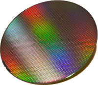
(Silicon wafer image courtesy of .RGB. / Flickr. Used under a Creative Commons CC BY 2.0 license.)