iFixit tears down Sony’s 42MP a7R II revealing its impressive interiors
posted Thursday, August 20, 2015 at 12:00 PM EDT
Sony’s a7R II is one of the most impressive cameras we’ve come across recently; and with good reason — it packs a lot of punch in a little design. Just what exactly is inside of that black little frame, though?
Per standard procedure, iFixit has gotten their hands on a production sample of the a7R II and for the enjoyment of all gear heads out there, they have torn down Sony’s a7R II piece by piece to see exactly what it is this mirrorless beast is made of.
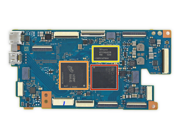
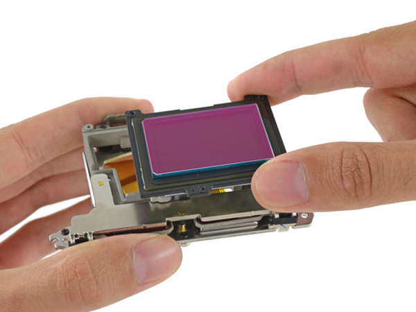
On their dedicated teardown page for the Sony a7R II, iFixit walks through every detail of the camera, from the processors that power the camera to its 5-axis SteadyShot image stabilization technology. We’ll leave the commentary to those of you interested in pointing out the intricacies of the camera, but we did notice one inconsistency in iFixit’s teardown.
In the words of our Editor-in-Chief, Dave Etchells:
In Step 18, iFixit says the 5-axis SteadyShot has ‘enough variety to adjust the sensor on five distinct axes’. That’s not actually correct; the sensor actuator can only move the sensor in three degrees of freedom: up/down, left/right, and rotate it about its center. The camera’s processor uses those three movements to compensate for camera motion along five axes, but the IS actuator only has three motions available to it.
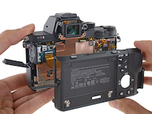
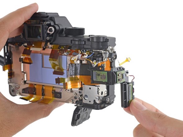
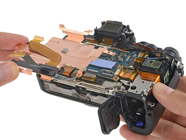
Below are a few shots of the teardown in process:
To check out the teardown in all its glory, head on over to iFixit’s a7R II page.
*Image credits: Images courtesy of iFixit