Panasonic’s global shutter technology uses organic film to increase sensitivity and reduce distortion
posted Monday, March 21, 2016 at 4:46 PM EDT
[Editor's Note: We meant to publish this article back in February, but just realized it never went live until we looked back for it while editing our CP+ Fujifilm executive interview, which also touches on this interesting technology. Apologies for the delay!]
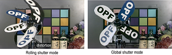
Back in February, Panasonic announced that they had developed global shutter technology for CMOS image sensors that uses Fujifilm-developed organic photoconductive film (OPF). Global shutter is shutter operation capable of capturing an image in all pixels simultaneously, in contrast to an ordinary CMOS sensor which uses rolling shutter to capture an image (exposure and shutter operation is performed one row after another). Rolling shutter is what causes the dreaded "jello effect" distortion due to camera shake, or the extreme distortion sometimes seen in rapidly-moving objects like airplane or helicopter propellers.
The new sensor technology also has up to 10x higher dynamic range, because it can accurately record much higher light levels without saturating or clipping highlights than conventional technologies that support a global shutter function.
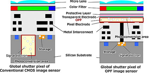
In conventional CMOS sensor technology, the photodiodes that convert light to electrons are also used to store the electrical charge that results. In order to implement a global shutter, additional space must be provided to offload the charge from the active light-sensing area, so it can be read out without being affected by new light arriving. The problem is, this charge-storage area takes up space that's then not available for sensing light, so you end up trading off light sensitivity. At the same time, and even more problematic, the photodiode can't collect and convert as much light without saturating. (Reaching a level at which the signal no longer increases with increasing exposure.) The amount of charge that can be stored in the separate storage area is also a function of its size, so it's a no-win compromise: No matter what you do, you're forced to give up dynamic range.
With the new organic photo-conductive film, light conversion and charge storage are separated, so there's no longer a tradeoff between the two. The light-sensing element can expand to cover basically the entire pixel area, and the charge-storage element can become much larger as well. The net result should be both improved light sensitivity and greater dynamic range, allowing the sensor to record brighter scenes without losing highlight data.
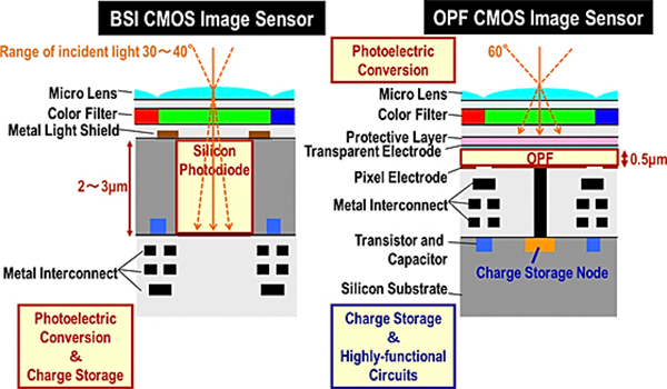
At the same time, the OPF expands the angle of incident light rays the sensor can respond to, because it lies at the very top of the stack of the pixel circuitry, directly beneath the microlenses and color filter array. It's basically a 2-D structure (only 0.5 micron thick, vs typical depths of 2-3 microns for conventional photodiodes) so it can respond to light across a very wide 60 degree range of angle of incidence, a good 20-30 degrees wider than most conventional CMOS sensor technology. This could potentially reduce problems of exposure uniformity and color shift between the center of the image and the edges, with lenses that are less than perfectly image-space telecentric.
While the basic structure of the sensor should lead to increased dynamic range, it seems that a significant amount of the claimed 10x greater dynamic range results from another Panasonic technology that allows per-pixel variable exposure timing. It's not clear to us just how this works without doing some digging into their patents, but the basic idea seems to be that they can use shorter exposures in bright areas of the image to prevent the pixels from saturating, while using longer exposure times in darker areas. (There are a lot of patents involved: Panasonic says they hold 60 Japanese and 41 international patents related to this technology.)
What's not clear in all this is how the basic sensitivity and noise levels of this technology compare to conventional sensors. Rather than capturing photons in the silicon photodiodes of conventional CMOS sensors, the OPF material is what does the conversion. What's not stated is what the conversion ratio is from incident photons to electrons captured on the charge storage elements. Also, what's the "dark current" like? (Dark current refers to minute leakage currents that occur in photodiodes even when there's no light falling on them. It's a component of the image noise we see at high ISO levels.)
Until we know more about the capabilities of the OPF film itself, it's hard to evaluate just how significant this new sensor technology really is. It's encouraging, though, to see companies exploring fundamentally different sensor technologies: Underlying material limitations mean there's not much more improvement to be found with conventional silicon photodiode sensor technology, so substantial improvements over the current state of the art are going to require fundamentally different approaches.
For more information on this new technology, including information on multiple exposure technology and additional diagrams, see Panasonic's press release here.
As noted, it's not clear how this new technology will ultimately stack up against conventional CMOS chips in terms of sensitivity and noise levels, let alone when it might find its way into consumer products. If noise and sensitivity can compete with conventional CMOS and fabrication costs are comparable, though, it could be a game-changer. It also will be interesting to see if and how Panasonic and Fujifilm might collaborate with each other on other new technologies.
(Dave Etchells contributed to this story. Seen via 4/3 Rumors)