PRESS RELEASE: Toshiba Corporation Launches Highly Sensitive CMOS Image Sensor With BSI
Applies world's first 300mm wafer lines for BSI technology
TOKYO, Japan., October 27, 2009 - Toshiba Corporation (TOKYO: 6502) today announced the launch of a new CMOS image sensor that will bring 14.6 million pixels to digital still cameras and to mobile phones supporting video imaging. The sensor, the latest addition to Toshiba’s “Dynastron™” line-up, is also the company’s first to integrate the enhanced sensitivity offered by back-side illumination technology (BSI). Sampling of the new sensor will begin in December and mass production will follow from the third quarter of 2010 (July--September).
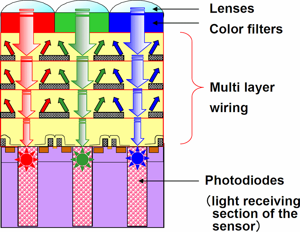
BSI brings new levels of responsiveness to CMOS imaging. Lenses are deployed on the rear of the sensor on the silicon substrate, not on the front, where wiring limits light absorption. This positioning boosts light sensitivity and absorption by 40% compared to existing Toshiba products, and allows formation of finer image pixels.
Toshiba has made full use of the advantages of BSI to realize image pixels with a pitch of 1.4 microns, and to pack 14.6 million of them into a 1/2.3-inch sensor that meets the high level imaging and processing requirement, and that will also bring a new level of image quality to mobile phones. Toshiba will use the new sensor to promote its full-scale entry to digital camera market, and will continue to develop BSI products as a mainstream technology.
The new sensor will be mass produced at Toshiba’s Oita Operations, on industry leading 300mm wafer lines deploying 65nm process technology. Initial production will be at a volume of 500,000 sensors a month.
CMOS image sensors are a focus product of Toshiba’s System LSI business. Until now, their main application has been in mobile phones, where Toshiba could leverage its high density integration and low power consumption technologies. With the introduction of BSI CMOS sensors, Toshiba will reinforce the sensor business by expanding application to include digital cameras.
 | 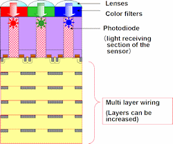 |
Conventional structure:FSI type
(Front Side Illumination)
Lenses are formed on top of the sensor, with wiring between them and the
light receiving section and photodiodes. Light entering the sensor obliquely is
blocked by the wires, which also reflect back some to the light that enters at
right angles, degrading overall light sensitivity. |
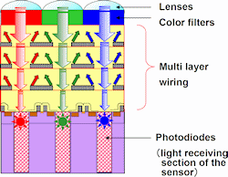
This structure: BSI type
( Back-side Illumination)
The lenses are attached to the back side of a substrate with a planed surface,
and deliver light directly to the photodiodes. With no interference from wiring, light sensitivity and overall performance are boosted. |
| Diagrams provided by Toshiba Corp. |
Key feature
| Optical format: | 1/ 2.3 inch |
| Number of pixels: | 14.6 mega pixels |
| Size of pixels: | 1.4 micro meter |
Frame rate: | 60 frame per sec. (Supports 1080p, 720p) |
Note: Dynastron is a trademark of Toshiba Corporation
*About TAEC and Toshiba Corp.
Through proven commitment, lasting relationships and advanced, reliable electronic components, Toshiba enables its customers to create market-leading designs. Toshiba is the heartbeat within product breakthroughs from OEMs, ODMs, CMs, distributions and fabless chip companies worldwide. A committed electronic components leader, Toshiba designs and manufactures high-quality flash memory-based storage solutions, discrete devices, displays, advanced materials, medical tubes, custom SoCs/ASICs, digital multimedia and imaging products, microcontrollers and wireless components that make possible today's leading cell phones, MP3 players, cameras, medical devices, automotive electronics and more.
Toshiba America Electronic Components, Inc. is an independent operating company owned by Toshiba America, Inc., a subsidiary of Toshiba Corporation, Japan's largest semiconductor manufacturer and the world's third largest semiconductor manufacturer (Gartner, 2008 WW Semiconductor Market Share Report, April 2009). For additional company and product information, please visit http://www.toshiba.com/taec/.
Information in this press release, including product pricing and specifications, content of services and contact information, is current and believed to be accurate on the date of the announcement, but is subject to change without prior notice. Technical and application information contained here is subject to the most recent applicable Toshiba product specifications. In developing designs, please ensure that Toshiba products are used within specified operating ranges as set forth in the most recent Toshiba product specifications and the information set forth in Toshiba's "Handling Guide for Semiconductor Devices," or "Toshiba Semiconductor Reliability Handbook." This information is available at http://www.chips.toshiba.com, or from your TAEC representative.
(First posted on Wednesday, October 28, 2009 at 22:38 EDT)