The following is an unedited press release, shown as received from the company represented. We've elected to present selected releases without editorial comment, as a way to provide our readers more information without further overtaxing our limited editorial resources. To avoid any possible confusion or conflict of interest, the Imaging Resource will always clearly distinguish between company-provided press releases and our own editorial views and content.
Company Enhances Aptina™ A-Pix™ FSI Technology; Plans Roll Out of BSI Solution
SAN JOSE, Calif.--(BUSINESS WIRE)--Underscoring its commitment to excellence in pixel performance, Aptina, the leading innovator of CMOS imaging technology, today detailed its strategy to address the challenges designers face as the industry moves toward smaller pixel sizes. Enhancements to the company’s third generation Aptina™ A-Pix™ frontside illumination (FSI) image sensor technology enable significant improvements in quantum efficiency (QE) and crosstalk and provide a 25 percent improvement in light level for the same signal-to-noise ratio performance over second generation technology. Today, the company also announced its plans to introduce backside illumination (BSI) image sensor technology in the second half of 2010 to address those applications requiring 1.1-micron pixels and below. With the combination of its industry-leading portfolio of high-quality imaging solutions, the enhancements to its Aptina A-Pix image sensor technology and strategy for BSI image sensor solutions, Aptina is well positioned to maintain a leadership position in the market. The company has also announced two new products today that integrate Aptina’s enhanced technology. (See release entitled Third Generation Aptina™ A-Pix™ Technology Enhances Mobile Imaging Solutions)
Despite industry trends toward higher resolution and smaller pixels in many imaging applications, there are also a growing number of applications requiring larger pixels with their superior low-light image quality. Applications such as HD video in digital still and video cameras, mobile phone cameras, PC’s and surveillance will require the excellent image quality enabled by larger pixel sizes, such as such as 1.4- and 1.75-micron, and these larger pixels favor FSI solutions such as Aptina A-Pix.
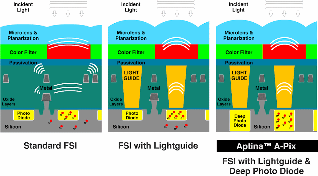
The new Aptina A-Pix advancements announced today extend the capabilities of FSI with a new wide lightguide and introduce deep photodiode technology. Aptina A-Pix leverages a new advanced semiconductor manufacturing process with 65 nanometer pixel design rules. This process allows for wider metal openings to insert larger lightguides into the pixel to channel more photons through interconnect layers, and efficiently capture them in the deep photodiode. The deep photodiode is a photodetector engineered to extend the depletion depth into the silicon wafer to capture electrons generated by long wavelength photons that would otherwise be lost to recombination or to adjacent pixels resulting in lower QE and crosstalk. Aptina has also enhanced the microlens and optical layers to maximize light collection. Not only do these enhancements improve FSI technology performance, they are also proving essential in the development of a market-leading 1.1-micron BSI pixel.
“Aptina is committed to being the preferred partner in developing and delivering distinctive imaging solutions rapidly and cost effectively to address the needs of our customers,” said Gennadiy Agranov, Vice President, Imaging Technology at Aptina. “Today, we are seeing a conflict in market requirements between the move toward smaller high-resolution cameras with smaller pixels and that of growing expectations for improved image and video performance. For these reasons, we believe our strategy to continue enhancing our industry-recognized FSI image sensor technology while introducing BSI technology for those applications with the very smallest pixels, is the best approach.”
About FSI and BSI With an attractive performance/ cost value proposition, FSI is the principal technology used in image sensors today, helping to drive the widespread adoption of cameras in cell phones, notebook computers, digital video and still cameras and numerous other applications. FSI is particularly well suited for applications like HD video that require “larger” pixels – where low light and overall imaging performance is critical. For high-quality HD video, 1.4- and 1.75-micron FSI pixels are expected to have a long life.
Early in its development, BSI technology is finding use in higher end consumer cameras where paying a premium for the sensor is less of a concern for the manufacturer. As future applications require 1.1-micron sensors, BSI is expected to be required as FSI may be unable to achieve the required performance.
For more information about frontside and backside illumination, download Aptina’s technology white paper, An Objective Look at FSI and BSI, or check out Aptina’s webcast at http://www.aptina.com/FSI-BSI.
Pixel structure of Aptina's third generation A-PIX frontside-illuminated CMOS sensor (right), compared to first (left) and second generation (middle) designs.. Image provided by Aptina Imaging Corp. / Business Wire.
About Aptina A-Pix Technology Aptina A-Pix is a series of advanced pixel technologies, featuring lightguide and deep photodiode, and 65 nanometer pixel design rules that cost-effectively advance pixel performance. The new, third generation Aptina A-Pix enhances quantum efficiency and minimizes crosstalk to capture sharp images with vibrant colors even in the low-light conditions that challenge traditional sensors. Aptina has already shipped millions of imaging products containing earlier generations of Aptina’s reliable and established FSI technology. Aptina A-Pix makes it possible for mobile phone cameras to capture quality images to compete with digital still cameras, and enables a new class of hybrid camera that combines digital still image capture with advanced high-performance HD video. Continuing with this success, Aptina is releasing a wide range of 1.4-micron products to leverage the latest advances in the third generation Aptina A-Pix technology. These new additions to the Aptina portfolio range from a high performing 14MP, targeted for DVC and high-end mobile phone handsets, to a 3MP sensor for mainstream mobile handsets.
About Aptina Aptina is a global provider of CMOS imaging solutions with a growing portfolio of products that can be found in all leading mobile phone and notebook computer brands as well as a wide range of products for digital and video cameras, surveillance, medical, automotive and industrial applications, video conferencing, barcode scanners, toys, and gaming. Aptina enables Imaging Everywhere™ and continually drives innovation in the market as seen with the introduction of the first 14MP CMOS image sensor for point-and-shoot and hybrid cameras (MT9F001), and the industry’s first 5MP SOC with ¼” format (MT9P111). Privately held, Aptina’s investors include Riverwood Capital, TPG Capital and Micron Technology. For additional information on Aptina visit www.aptina.com or subscribe to the latest news from Aptina by copying the Aptina RSS feed into your favorite RSS reader.