Sony ramps up smartphone CMOS sensor production
posted Friday, June 22, 2012 at 2:50 PM EDT
 Worldwide, sales of smartphones are soaring, and that means an increasing demand for the tiny image sensors that form the heart of the multiple cameras found in a typical smartphone. Responding to that demand, Sony Corp. has today announced plans to invest another 80 billion yen (close to US$1 billion) in a semiconductor facility in Fukuoka, Japan.
The new cash injection follows hot on the heels of last year's 100 billion yen investment in the same facility, which was used to double its CMOS image sensor production. In part, the additional funding announced today will allow Sony Semiconductor Corp.'s Nagasaki Technology Center to procure wafer processing equipment for production of stacked CMOS image sensors, more commonly known as backside-illuminated sensors. These place the supporting circuitry for each pixel location on a separate layer beneath the pixel, rather than alongside it, allowing a greater area of the sensor surface to be devoted to light gathering. The company also intends to invest in converting existing equipment at the facility for use in CMOS sensor manufacturing, as well as increasing its wafer output.
Around 45 billion yen will be invested in the Nagasaki Technology Center during the current fiscal year ending March 2013, and the remainder by the end of September 2013. At this point, Sony's total production of CCD and CMOS image sensors would be around 60,000 wafers per month. More details in the press release below...
Press Release
Sony increases production capacity for stacked CMOS image sensors
- Increasing total production capacity for image sensors to approximately 60,000 wafers per month to supply image sensors mainly for smartphones -
June 22, 2012, Tokyo, Japan – Sony Corporation ("Sony") today announced that it plans to invest in Sony Semiconductor Corporation's Nagasaki Technology Center ("Nagasaki TEC") from the first half of the fiscal year ending March 31, 2013 through the first half of the fiscal year ending March 31, 2014, to increase the production capacity for stacked CMOS image sensors.*1
This investment is intended to provide for new wafer processing equipment for stacked CMOS image sensors, and to increase and transform wafer lines capable of manufacturing CMOS image sensors. With this development, Sony plans to increase total production capacity for CCD and CMOS image sensors to approximately 60,000 wafers per month by the end of September 2013.*2
In light of the rapidly expanding demand for smartphones and tablets, Sony plans to continue to solidify its leading global position in CMOS image sensors by strengthening its production capabilities for stacked CMOS image sensors, which provide greater performance in a more compact form. Furthermore, Sony intends to accelerate its growth strategy by incorporating superior core technologies, including stacked CMOS image sensors, into a wide range of products for its digital imaging and mobile businesses, which are priorities within its electronics business.
The investment amount is approximately 80 billion yen, of which, the amount to be invested in the current fiscal year ending March 31, 2013 (approximately 45 billion yen) was included in the forecast of the capital expenditures for semiconductors in the current fiscal year announced at the annual earnings release on May 10, 2012. In addition, Sony will utilize a governmental subsidy in its investment plan which will be provided by the Ministry of Economy, Trade and Industry in Japan, through the "Subsidy for Domestic Location Promotion Projects" program.

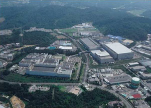
Sony Semiconductor Corporation's Nagasaki Technology Center
*1: CMOS image sensors in a stacked structure layer the pixel section containing back-illuminated structure pixels onto chips containing the circuit for signal processing, in contrast to the supporting substrates used in conventional back-illuminated CMOS image sensors. These products enable Sony to mount large-scale circuits while decreasing the chip size of image sensors, thereby enhancing image quality and functionality and allowing for a more compact size for digital cameras and mobile devices.
*2: This total production capacity (300mm wafer basis) includes the output of foundry operations to which Sony outsources a part of the manufacturing process. For the purposes of calculating total production capacity, the capacity of 200mm wafer production lines in Kagoshima Technology Center and Nagasaki TEC is converted to the new 300mm wafer production capacity basis.
|
Purpose of Investment:
|
Increase production capacity for stacked CMOS image sensors
|
|
Investment site:
|
Sony Semiconductor Corporation, Nagasaki Technology Center (Isahaya-shi, Nagasaki Prefecture)
|
|
Investment details:
|
* Nagasaki TEC Fab 2 facility: installing equipment to manufacture CMOS image sensors and part of wafers lines.
* Nagasaki TEC Fab 3 facility: transforming certain existing equipment to manufacture CMOS image sensors. * Nagasaki TEC Fab 4 facility: installing and increasing part of wafers lines. |
|
Investment time frame:
|
From the first half of the fiscal year ending March 31, 2013 through the first half of the fiscal year ending March 31, 2014
|
|
Investment amount:
|
Approximately 80 billion yen
Of which, the amount to be invested in the current fiscal year ending March 31, 2013 (approximately 45 billion yen) was included in the forecast of the capital expenditures for the current fiscal year announced at the annual earnings release on May 10, 2012. |
|
Outline of Sony Semiconductor Corporation
|
|
|
1. Head office:
|
2-3-2 Momochihama, Sawara-ku, Fukuoka-shi, Japan
|
|
2. Establishment:
|
April 1, 2001
|
|
3. Representative Director (President):
|
Masanori Okayama
|
|
4. Capital:
|
24.25 billion yen, fully owned by Sony Corporation
|
|
5. Production Bases:
|
Kagoshima, Oita, Nagasaki, Kumamoto, Shiroishi-Zao (Miyagi) and Higashiura (Aichi)
|
|
6. Number of employees:
|
Approximately 7,300 (including contract and temporary employees) as of April 2012
|
|
7. Business Activities:
|
Development, design and production of semiconductors
|
|
Outline of Nagasaki Technology Center
|
|
|
1. Location:
|
1883-43, Tsukuba-machi, Isahaya-shi, Nagasaki, Japan
|
|
2. Establishment:
|
December 1, 1987
|
|
3. Representative Officer (Nagasaki TEC President):
|
Yoshihiro Yamaguchi
|
|
4. Site area:
|
194,000-square-meter
|
|
5. Floor area:
|
221,000-square-meter
|
|
6. Main products:
|
CMOS image sensors and MOS LSIs
|