Inside Sony Kumamoto: A rare glimpse inside Sony’s super-secret sensor factory
posted Tuesday, September 5, 2017 at 11:05 AM EDT
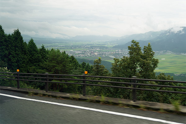
Back in early August, I had the very rare opportunity to tour Sony's sensor factory in Kumamoto, Japan. We had only limited access to the factory itself, but I learned a lot about Sony's sensor technology and fabrication process while I was there, and will be sharing more on the topic in other forthcoming articles. In this first piece, we'll look at a few of the intriguing parts of the sensor production process.
We weren't allowed to take photos ourselves of the factory floor, given the extremely proprietary nature of the wafer processing. I can understand the need for such caution, given my own time in the semiconductor industry, albeit many years ago. Even seemingly innocuous details in a photo could reveal important aspects of Sony's process to competing production engineers who know what to look for. Instead, Sony provided us with a collection of their own photos, that had been carefully screened and cleared for public dissemination.
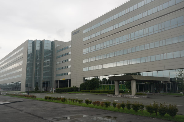
Even with the limited access, it was a very interesting glimpse into how the sensors in so many of our cameras are made. (Sony holds a dominant position in the global sensor market. There's a better than 50% chance that the sensor in your current camera came out of this factory.)
This is where the whole process begins, outside of Sony's factory at a company that grows the raw silicon. "Grows" is a literal description, because the silicon wafers are sliced from massive, single crystals of silicon.
These large lumps of silicon are called boules, and at the current state of the art are absolutely enormous. The finished wafers are about 12 inches (300 mm) in diameter, by perhaps 4 to 6 feet long (1.4 - 2 meters). The large boules are produced by melting a large amount of very pure silicon, holding it very close to its freezing (crystallization) point, and then dipping a small, precisely-oriented seed crystal into the top of the melt.
With careful control of the temperature, the molten silicon will begin crystallizing around the seed crystal, growing a single crystal with the same orientation as the seed. The seed crystal is slowly pulled up and away from the melt, while being rotated to help maintain uniformity as the crystal grows.
This technique is called the Czochralski process after the Polish scientist Jan Czochralski, who invented it in 1915, and is how most semiconductor-grade silicon is made today. The process is much the same as you might have observed when crystallizing sugar to make rock candy. There, multiple nucleation sites make for a multitude of crystals; when growing silicon, a single seed crystal and careful control results in just one monster crystal.
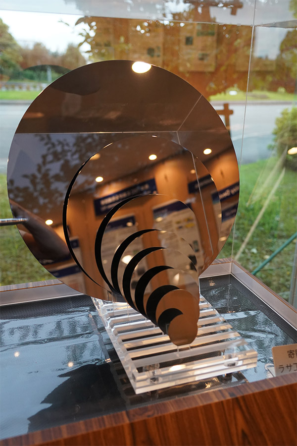
Silicon wafer sizes have gotten a lot larger over time, because larger wafers make for more efficient processing and thus cheaper chips. In the early 1970s, 3-inch wafers were standard, now 12-inch (300mm) wafers are commonplace, and manufacturers continue working to increase sizes even further. At less than a millimeter thick, today's wafers are pretty fragile, requiring careful handling.
All this happens at the silicon supplier, who then slices the boules into thin wafers, again unspecified by Sony, but the standard thickness for a 300mm wafer is 0.775mm. (This gives you some idea of how carefully they have to be handled. Imagine a 12-inch disk of brittle material, less than 1mm thick. Oh - and you can only grab it by the extreme edges!)
The huge (roughly 12 inches in diameter) silicon wafers arrive at Sony's Kumamoto factory in special carrier boxes that protect them during transit from the silicon provider, avoiding breakage and keeping them reasonably clean relative to the surroundings.
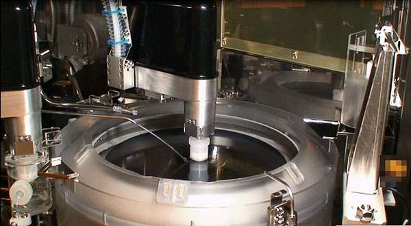
"Reasonably clean" isn't anywhere near clean enough to be allowed to enter the factory environment, though, so the first step in their journey is the liquid cleaning station shown above. Here, they're removed from the incoming carrier box, and placed on a spinning stage. As the wafer spins, high-purity water is squirted onto it, and a rotating scrubber moves from the center to the edge and back again. When done, the scrubber retracts, a final jet of water is applied, and then the wafer is spun at high speed to sling all the water off the edges, leaving a pristine surface.
A mechanical handler then picks up the wafer and transfers it to a different, ultra-clean carrier box that is used to carry batches of wafers from one station to the next, via the factory's automated material-handling system.
Circuit patterns are made on the wafers using a photolithography process. This happens dozens of times throughout the sensors' production cycle, to define patterns for different parts of the process. In some cases, the patterns control where "dopant" atoms will go, to turn the raw material into N- and P-type silicon. Sony's sensors have quite complex structures, and each structure requires its own photolithography step.
In photolithography, the wafers are coated with a thin film of photo-sensitive material known as a "photoresist". An image of the desired pattern is projected onto the wafer's surface and the image is developed, leaving some areas covered by the resist and others clear. Interestingly, there are both "positive" and "negative" resists, meaning that the exposed portion either stays or is removed during the development process. Way back in semiconductor pre-history when I was in the IC business, positive resists had higher resolution, but I have no idea what resist technology is like these days. Sometimes the resist acts as a mask for the ion-implantation process (see below), while other times, the resist is applied over a continuous metal or layer, with the resist patterns determining what metal/oxide will be etched away and what will be left behind.
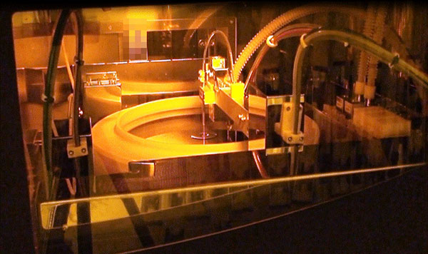
The first step in the photolithography process is to apply the photoresist in an incredibly thin, uniform layer, all across the wafer's surface. That's what's being done above, and if the setup looks a lot like the liquid cleaning station we saw first, it's because the main piece of equipment is the same sort of spinning stage as we encountered there. Here, a small amount of liquid photoresist is applied to the center of the wafer, which is then spun at very high speed to produce a microscopically-thin film.
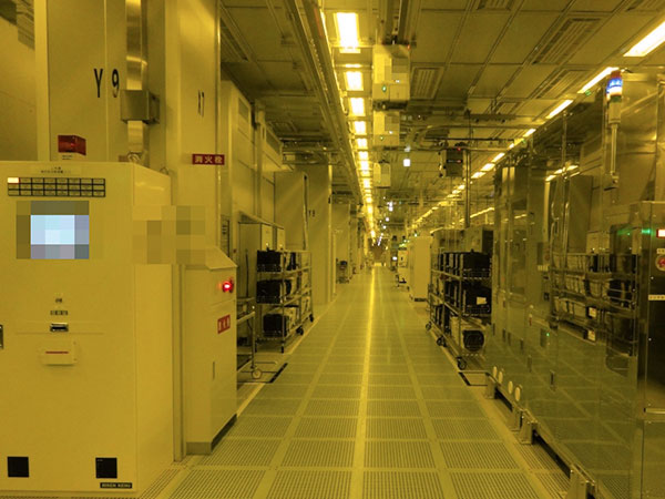
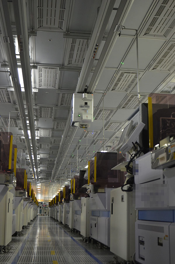
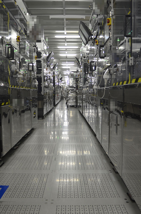
This is a view down one aisle of the Kumamoto factory's massive clean room area. We don't have a number from Sony for the total square footage of clean rooms, but the factory buildings are massive, and two entire floors are clean room space.
That's not all, though, because it takes three other floors to support one clean room level. An entire floor above the clean room is dedicated to air supply, and an entire floor below the clean room is air return, to be cleaned and recirculated again. Below the air-return floor, on the first floor of the building is a machinery level, with pumps, water filtering, etc, to support the clean rooms above. (I'm not sure, but I think that the first-floor machinery supports both the 3rd and 6th-floor clean room areas.)
It's no surprise that clean rooms are all about dust control. The main clean room area here is actually fairly "dirty" as such standards go, being a Class 1000 environment. That means there could be up 1000 particles larger than 0.5 microns per cubic foot of air. That sounds like a lot, but it's about 35,000 times cleaner than typical city air.
The really clean areas are inside the processing machines themselves, and inside the so-called FOUP wafer-carrying boxes that are automatically carried throughout the plant via a track system hanging from the ceiling. These smaller areas are rated Class 1, meaning no more than 1 particle larger than 0.5 microns in size per cubic foot of air.
I'm not sure, but I think that this particular aisle is one that we looked down when we were at the factory, and it contains ion implanters, diffusion furnaces and photolithography systems. Basically, it's an area where the dopant atoms are implanted in the silicon to make electrically-active areas with different characteristics.
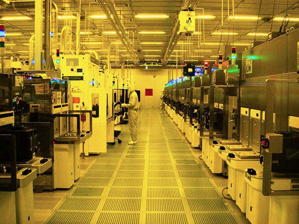
Here's a shot of another clean room area; I think this one is mainly photolithography, or perhaps etching of some sort. You can see one of the wafer-carrying robots in this shot, protecting a load of wafers in their ultra-clean internal environment as they're transported between machines.
This shot and the one above are actually a little unusual, in that there are people present. The Kumamoto factory is almost completely automated, with humans rarely even being in proximity to the wafers. The factory workers' duties seemed to be almost entirely limited to servicing, tweaking and repairing the production equipment itself. Other than that, most operations in the factory run 24/7 without human intervention.
The extreme level of automation is key to keeping costs down and production high. Humans are problematic in semiconductor production. Even outfitted in "bunny suits", they're incredibly dirty, shedding dust and skin cells everywhere. They also get tired, get sick, have bad days and just by their nature make mistakes from time to time, no matter how careful they are. Oh, and you have to pay them, give them vacations and benefits, etc, etc.
By contrast, the robot assembly line cranks day and night, never gets tired or sick, and always does things exactly, precisely the same way. (Thanks, robots, for our incredibly affordable sensors, relative to what they can do! :-)
This shot clearly shows a FOUP wafer container being carried by one of the overhead robotic trolley cars. When a trolley reaches its destination machine, the FOUP is lowered down on what looked like steel rods, but which obviously must have been telescoping tubes, to have fit within the body of the carrier robot. It was surprising to see how far down the FOUPs were lowered; depending on the machine involved, I'd estimate that they were lowered down a good 6-8 feet below the trolley car. It seemed a little precarious, but I guess with no clumsy humans around to blunder into a dangling FOUP, the setup didn't need to be especially robust.
During the huge Kumamoto earthquake, many FOUP-trolleys and the FOUPs themselves came crashing to the floor, and in some areas, the entire ceiling collapsed. It's almost unbelievable that the entire factory restarted for limited production in just a month and a half, and was back to full operation just seven months after the quake.
You can also see the alternating grid of air outlets, covering the entire ceiling of the cleanroom area. As mentioned earlier, the entire floor above the cleanroom is dedicated to air supply and filtering. Given the area involved and the need to main a continuous flow of ultra-clean air, the total airflow must be absolutely enormous.
You can also clearly see the grid of holes in the floor that the air exits through. Any dust particles kicked up from the floor the few times humans are present will just be sucked right down into the air-return system.
I don't know what's going on in this shot, as Sony was extremely guarded and cryptic about anything having to do with the production details. (Although I suspect any semiconductor process engineer would immediately recognize these machines for whatever they are.) Sony just described this area as being for the "photolithography process".
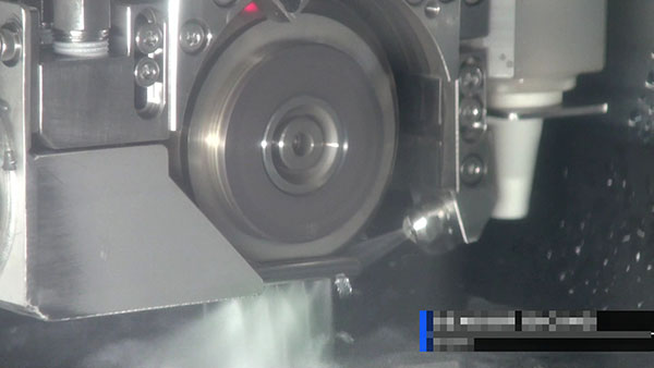
Once the sensor chips have been fabricated, they're subjected to wafer-level tests, then sliced into individual chips. This is called "dicing", and because silicon surface area is such a precious commodity, it's done with extremely thin-kerf diamond saws. (The "kerf" is the width of the slit they leave behind.) The specs for these kinds of saws and blades are pretty astonishing. A typical blade might be only 20-30 microns thick (0.02-0.03 mm or just 0.008-0.012 inches), and spin at 30,000 - 60,000 rpm to maintain stiffness and minimize silicon damage. Multiple nozzles spray high-purity coolant at the blade and wafer during cutting, to keep the saw and wafer cool, and also to carry away the microscopic silicon particles that are cast off.
For ordinary sensors (that is, ones which aren't stacked with memory/processor chips the way that the ones in cameras like the Sony A9 and RX100 V are), the next step is to mount them in packages and then bond incredibly fine wires to them, electrically connecting the contact pads on the chip to the pins of the package. The shot above shows a wire-bonding machine in action, but it hardly gives an appreciation for how fast they are. Time is money, so the more chips per hour a wire-bonding machine can process, the better.
We don't have any details on the type of wire-bonding machines Sony uses in their Kumamoto plant, but the video above gives you some idea of just how quickly they can move. Besides the direct point-to-point wiring the machine in the video is doing, some applications and packages require the machines to perform a complex dance after the wire is initially bonded to the chip, bending it into the right shape to clear chip or package geometry before bonding it to the package. Keep in mind, too, that even at these incredible speeds, the wire bonder needs to hit the pads on the chip with an accuracy on the order of 0.001 inches (~50 microns or less). The combination of temperature and pressure the machine uses to make the bonds also has to be very tightly controlled; even a failure rate of 0.001% would be disastrous for sensor yields.
This shot shows a loooong double-row of Sony's in-line sensor assembly machines. Processed sensor chips and empty chip packages go in one end, and finish-packaged sensors come out the other.
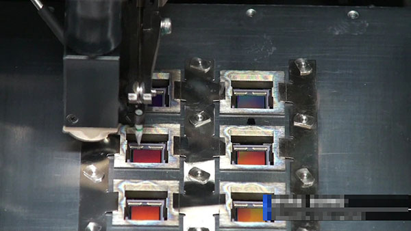
There are a number of steps involved in packaging sensor chips, all done within these integrated systems. Once the wafers have been diced, each sensor die is glued (yes, glued) into a package, using four drops of special resin. (Some kind of epoxy, I think?) Next, it's connected to the pins of the package via the wire-bonding step just described above. Then the package is filled with sealing resin, a cover glass is placed atop it, and the sealing resin is cured with a blast of ultraviolet light. Then a laser-engraving system marks part numbers, etc., onto the backs of the packages, they're sent for a final image-quality test, packed in shipping containers and warehoused before shipping.
The first-stage tests performed at a wafer level checked for raw electrical characteristics, while the second test after packaging verifies each sensor's imaging capability. I don't know how long the imaging test takes, but we were shown a huge room that was filled with second-stage image testing machines. Once again, we weren't allowed to share any photos, but the sheer scale of Sony's Kumamoto plant is mind-boggling.
Imaging parameters that are tested include dark current (basically, leakage current in the sensor's photodiodes that contributes to fixed-pattern noise in very dark conditions), low light performance, high-brightness performance and overflow handling (checking how the sensor behaves in the face of severe light overloads). And of course, they check for dead or stuck-high pixels as well.
Conclusion (for now)
That's it for this mini-tour of Sony's sensor production line. Next up will be a similar look at the production process for micro-OLED displays, of the sort used in the electronic viewfinders of cameras like the Sony A9, which are also produced in this factory. It's coming up on crazy-season for me here at IR, but I hope to also write a more detailed description of the processes involved in making a sensor. So many parts of it are familiar to me from my own time in the semiconductor business, even though that was decades ago now. Today's technology is enormously more advanced, but the basic steps are pretty much the same, and I'd love to be able to share some of the magic of how it all happens.
Meanwhile, do you have any questions about any of the above? Leave them in the comments below, and I'll try to circle back over the next few days to answer any that I can.