Photokina Q&A: Can the Samsung NX1 redefine pro performance with a quantum leap in technology?
posted Saturday, September 27, 2014 at 3:34 PM EDT

6.7 Billion pixels per second image readout? Check. 240fps hardware-based object-recognition and tracking? Check.
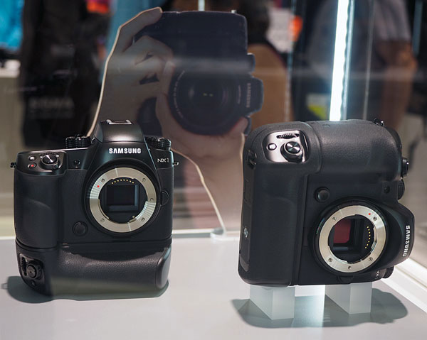
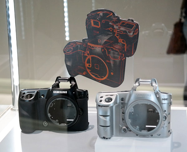
Without question, the Samsung NX1 was truly one of the standout products at the Photokina 2014 tradeshow in Cologne, Germany, with top-notch performance, a sophisticated hybrid autofocus system, and an amazing "auto-shot" mode that can capture a baseball in flight at the exact moment it's coming off the bat.
With its amazing speed and rugged build quality, the Samsung NX1 is clearly aimed at attracting professionals to the NX-mount, and it just might do that, if it tests as well in the lab and in the field as it shows in the tradeshow booth.
During the show, Imaging Resource publisher and founder Dave Etchells met with Samsung Electronics senior marketing manager for digital imaging, Jay Kelbley, for a wide-ranging discussion of the Samsung NX1, its cutting-edge technology, and why the company feels its offering to be unique in the marketplace.
What followed was a fairly technical discussion of just what Samsung has managed to pack inside the NX1's diminutive body, and some of its capabilities are pretty eye-popping. Read on for the details:
Dave Etchells/Imaging Resource: As you'd expect, I have a lot of questions about the Samsung NX1 and the technology in it, starting with autofocus. You make some really impressive claims for autofocus speed and capability, but on-chip phase detect isn't free of trade-offs. I wanted to talk about some of those and how Samsung's addressed them, or to what extent.
Jay Kelbley/Samsung Electronics: Sure.
DE: One obvious thing is that PDAF involves shading some of the pixels so they see light coming from just one side of the lens or the other. It's not a big problem, you can always bump up the gain in that pixel to compensate for the half of the light it's not seeing, but you guys have got a huge number of pixels and they're also cross-points.
JK: Sure.
DE: At what point or when does it become an issue with image quality, having so many focus pixels? Another way of asking that is what percentage of the pixels really are focus pixels?
JK: Well, even when you've got more than 200 phase-detect points, compared to 28 megapixels total, the percentage of AF pixels is miniscule.
DE: Ah, OK.
[Here's a little back-of-the-envelope, are-we-in-the-right-ballpark math to illustrate this: Let's assume that each focus point uses 500 pixels in each direction, or 1,000 pixels total. That'd mean 200,000 pixels across the sensor, out of a total of 28 million, or just 0.7%, and my assumption of 500 pixels in each direction is almost certainly overly generous.]
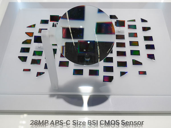
JK: As we're going up in resolution, we have some advantages relative to current sensor technology in fill. Our fill efficiency is much higher than most of the industry, thanks in large part to moving to 65nm design rules for our latest sensor.
[A nanometer (nm) is one billionth of a meter (10^-9 meters), or one millionth of a millimeter. While things like memory circuits have even smaller design rules, 65nm is unusually small for a sensor chip.]
DE: But it's backside-illuminated, so it's collecting all the light anyway.
[The point of this comment is that Jay was talking about smaller design rules (minimum feature size on the sensor chip) as contributing to a higher fill ratio, or percentage of the silicon area that's able to collect light. This was confusing, because as I had understood it, the whole point of BSI is that all the peripheral circuitry doesn't matter, so you could theoretically get a 100% fill factor. If that's the case, why would smaller design rules be a benefit here? Read on for the answer.]
JK: It's collecting all...
DE: So with the smaller design rules, you've got a bigger capacitor, essentially, to store it on? Is that what it is? Or a bigger potential well?
[Again, I was trying to understand what the consequence of smaller design rules meant. I was wondering if it meant they were able to create a potential well that could hold more electrons, which would contribute to lower noise levels.]
JK: Well, we can make much more efficient structures, smaller structures, so the net result is we can get better fill in general. We don't have to make big, thick walls on everything. As well, when we switch to copper [replacing polysilicon for the wiring on the chip], we've moved to a much more conductive material, which helps us in heat dissipation, it helps us in...
DE: Propagation of the signals across the chip? [Meaning potentially faster readout speeds]
JK: ...reducing resistance. So we're using less material, so again, even though we're BSI, we're cutting the pixel depth even more that way, which gives us more sensitivity and efficiency. So you'll find when you actually get these to test that the high ISO noise on these is much lower than it should be, if you follow the curve down in terms of pixel pitch, because of BSI, because of copper, because of the more efficient microlenses we've put on. The microlenses on these appear to cover almost 100%.
If you looked at the NX30 microlens, you'd say it looks to have 95%-ish coverage. For a square microlens it's pretty good; these things look visibly to be very close to 100% when you look at them on a microscope cutaway. So we're still making lots of incremental improvements and we're making them in technology vectors that no one else is. As far as I know, no other camera manufacturer is running a copper process for their sensors, and I don't believe any are running design rules close to these. I believe that some manufacturers, making higher-end cameras, are still running their processes in the range of 300nm design rules.

|
Copper metallization has been around the IC industry for years now - the photo at left is courtesy IBM Corporation, circa 1997.
Because copper is 40% more conductive than aluminum, it can increase circuit speeds and reduce power consumption. As far as we know, Samsung is the first sensor maker to use copper metallization. This contributes to the NX1's amazing speed, and the ability to track fast-moving ojbects without melting the sensor in the process :-) |
DE: By semiconductor standards, that's enormous.
JK: That's really large, and for memory structures, for computing structures, you can be down in the teens. So it's my understanding that we have the tightest design rules of any sensor manufacturing process used for cameras by a factor of two, and by general average probably close to a factor of four or five.
DE: It's interesting what you had mentioned, you know, you were talking about the "big thick walls". I just realized you were talking about the isolation diffusions between the pixels not taking up as much space with the smaller design rules, so even when you look at the backside-illuminated structure -- I'd been thinking that you've got 100% of the surface area available, but you still have to separate the photodiodes from each other, and that's where the smaller design rules come in.
The NX1's combination of larger pixels, smaller design rules, and reduced well depth accomplish the same effect, without the added complexity of the vertical light barrier.
JK: Right. Well, and you don't need as much material because the well depth is so much shorter as well. That being said, this isn't an ISOCELL process, so we're not putting in a reflective side layer which we don't need, again, because it's the short well depth.
[I think Jay might have used "well depth" at other points in the discussion to mean the front-to-back thickness of the diffusion defining the photodiode -- basically, the thickness of the silicon. In this case though, it's clear he's talking about the distance from the optical top of the stack of microlens, color filter array and any other structures to the photosensitive silicon surface.
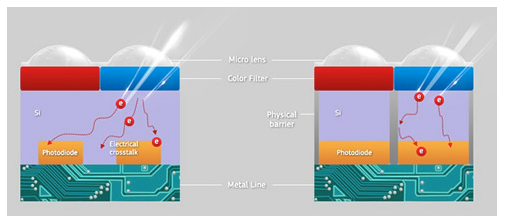
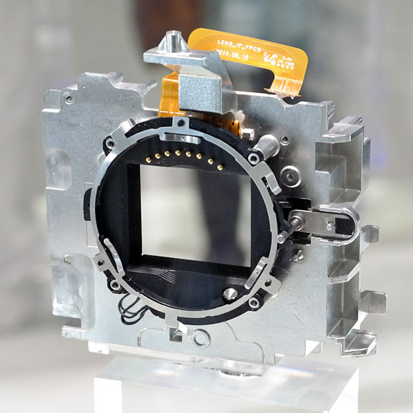
The Samsung's ISOCELL sensor tech that Jay's referring to here is a combination of backside illumination and physical separation of the pixels from each other, to prevent light from leaking between adjacent pixels. This "crosstalk" can reduce resolution and cause problems with color purity. Samsung first introduced ISOCELL technology in cell phone sensors having tiny 1.4 micron pixels. For whatever reason the structures above the silicon in the NX1's sensor appear to be thinner than was the case in chips using ISOCELL, so there's less chance for crosstalk to occur. Crosstalk would be less of an issue, though, due to the larger dimensions of the NX1's pixels. At roughly 3.6 microns vs 1.4 microns for the cell phone chip, the percentage of the photodiode area subject to crosstalk would be much less.]
DE: So even with BSI, there are some structures on the back of the chip still?
JK: Some structures...
DE: Because the well depth you're talking about, the... are you talking...
JK: Distance to the photodiode from the...
DE: From the surface. But if it's on the back, then I would think all the structures are on the front.
JK: You still have a CFA (color filter array), you still have some insulating layers, so there's still some depth there.
DE: There's still some depth there.
JK: I'll show you some illustrations out on the floor that'll show you that the well depth's about a third of what it is for front-side illuminated. Or not the well depth, but I'd say the light depth, so if you include the microlens in there, if you include the bonding layers, all that stuff, you're looking at probably less than a third of the distance that you'd have on a similar structure, frontside-illuminated.
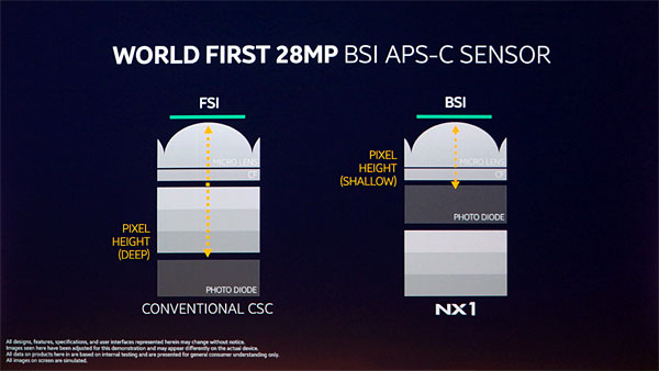
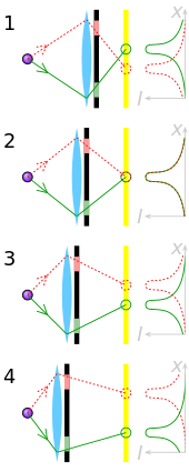
DE: Yeah, and so there are other advantages to BSI as well, because it's very shallow, in terms of the angle of incidence of light rays it can accept from the lens.
JK: Yes, it makes the microlenses much more efficient. You're looking at about a 70% improvement in angle of light to the photodiode.
DE: Wow, 70%. That's really significant.
JK: Versus the sensor that's in the NX30.
DE: Yeah. Now to some extent, the angle of the light, that's a function of the lens, what it's designed to put out in terms of the angle of the light rays that approach the sensor. But this might give you less shading, around the edges?
JK: Well, yes and no. That's up to the lenses that you're feeding the pixels with. It gives you an opportunity to use lenses that are less image-side telecentric...
[Telecentricity refers to how close light rays coming from the lens are to perpendicular as they contact the sensor.]
DE: Yeah.
JK: So in the last... long time, the last ten years-ish or so, as manufacturers have been building more digital lenses, they've been focusing on supporting microlenses with image-side telecentric light presentation...
DE: Yeah.
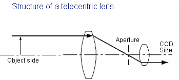
Image courtesy Keyence Vision Systems.
JK: You don't necessarily have to do that, you don't have to do that as much with this lens. You're not going to get the falloff, you're not going to get some of the color fringing that you get from bleed between pixels, and CFA pollution. That being said, most of the lenses that are on the market now, especially the ones from us, have been designed to already present the light relatively straight to the surface of the image sensor, so if it's already presenting the light straight that's fantastic with these backside-illumination structures, and it makes them even more efficient at collecting light.
DE: And I guess if this BSI technology propagates across the NX line, then that would give your lens designers more latitude too, in that they don't have to be constrained by the need for telecentricity?
JK: It could. I don't know that we'd take that opportunity, though. All this work that's gone on in the last few years across the industry in making the lenses better is still the right way to go, and I would assume and hope that that's the way most of the industry continues to go.
DE: Getting back to trade-offs with on-chip phase-detect AF, one of the big differences between the on-chip phase-detect and the conventional separate phase-detect sensors is that the conventional sensors have much larger pixels, and are consequently more sensitive to light compared to on-chip PD elements. So there's a tradeoff in light sensitivity if you go to on-chip. What's the low-light limit for the NX1?
JK: I believe it is rated to EV-4 for contrast and EV-2 for P.D. But the tradeoff isn't in the size of the phase-detect sensors, as you move from off-chip to on-chip. It comes in wavelength. So with the DSLR phase-detect sensors, you can run those wide open. You can run them into infrared, and that's what most designers do. So if you look at DSLR autofocus assist lights, many are running red-infrared, which is less obtrusive. The autofocus assist lights are generally red-infrared, but if you go on-chip you have the IR blocking filter on the image sensor, so on-sensor you can't use IR sensing for autofocus any more.
DE: Ah!
JK: Make sense. Because you're blocking the IR.
DE: Yeah, obviously, yeah.
JK: And so, the right strategy for on-chip AF assist ends up being visible spectrum, or in our case we've been using green lights for a long time. Now, the green light that's in this one for AF assist is the most powerful AF assist light I've ever seen; it's good out to 15 meters.
DE: Wow.
JK: We've also added in a pattern...
DE: Yeah, it has that patterning; perhaps using a holographic grating or something to project the pattern.
[Sony used a holographic grating to project an AF pattern a few years back, but it didn't persist in their product line. The reason I'm thinking they might be using a holographic grating to project it is that the pattern seems to stay pretty sharply-focused, regardless of the distance it's being projected.]
JK: It's a line pattern, let me see if I can dial that up. Here, look at this, Dave. If you look at the back of your computer actually. [He's projecting the AF-assist pattern on the lid of my MacBook.]

DE: Yeah, it's got a whole bunch of vertical lines, both broad lines and fine lines. Presumably the broad lines help when the camera's more out of focus, and the fine ones help it focus finely, once it's close ...
JK: Well, if you're in total darkness, you need a pattern.
DE: Yeah.
JK: Total darkness on a flat surface.
DE: Right, the projected pattern means you're not dependent on the surface that you're aiming it at.
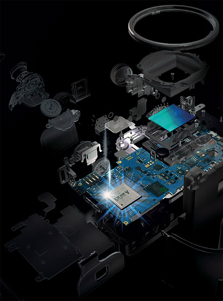
DE: When we were talking previously, you said that the architecture of DRIMe V is very different than DRIMe IV. What sorts of changes are made between them?
JK: The biggest change is the structure of the Image Signal Processor. The DRIMe V ISP is very different. Most ISPs have key parts of the processing hardwired to get the needed speed. What's really new with the DRIMe V is that the "hardwiring" can be reconfigured.
DE: That sounds very significant, although I have to admit I don't know how common it is that ISPs are actually hardwired.
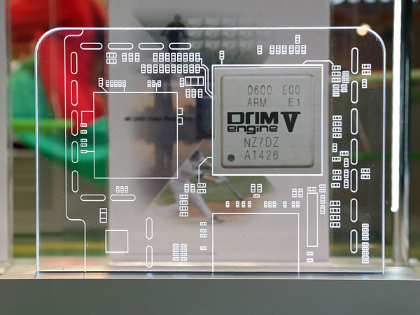
(Don't be confused by the mention of "ARM" on the chip. It does have no fewer than 5 general-purpose ARM processing cores, but its real magic comes from the hefty array of hardwired image-processing modules it contains.
JK: There's not much variability in them. Sometimes you'll get thresholding changes and small numeric variables, but the image path is usually very locked down...
DE: It's pretty much, a fixed pipeline.
JK: With a few tuning pieces, yeah.
DE: Whereas this is more configurable.
JK: Yes.
DE: And it's configurable not at the level of changing a firmware program, but you're actually changing the hardwiring. There are switches you can use to change the configuration of the functional units?
JK: Yeah, basically. And Samsung's software people are all over it; they're pretty sharp and I believe that we're really going to be able to tap fully into the DRIMe V's capabilities for the NX1.
DE: So even though it's hardwired, some of the connectivity is programmable through the firmware, so we can actually look for continued "firmware" development that would continue to improve performance, including the parts that are implemented in hardware.
JK: Yes.
DE: So there may be significant improvements in the near future. That's pretty interesting, because it sounds like it's already starting out pretty capable.
JK: And not just image quality, there's a lot going on in terms of programmability, like we talked about Samsung Auto-Shot mode before. Here's the UI for it.
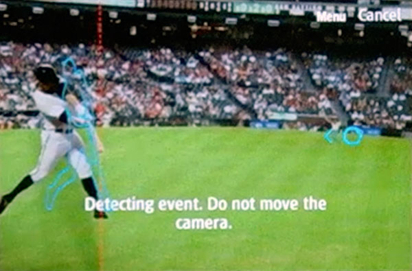
The outline of the batter is just illustrative, the important part is the vertical red line on the left. The camera tracks the ball at 240 frames/second, measures its speed, and predicts when it will reach the red line.
DE: Ah - I'd been wondering what it looked like!
JK: But that's, you know, a perfect example of using that DRIMe V image processing. It does motion tracking at 240 frames per second, using hardware-based object recognition.
DE: And did I read somewhere that it's not just tracking the baseball, but it's actually watching the bat as well?
JK: No, just the ball reaching that position. The development team is working on things like that, but currently the hardware is just tracking the ball. What's important to understand, though, is that this is all happening in hardware; that's the way we can track something that fast.
DE: Really? Oh!
JK: Yeah, every four milliseconds, the DRIMe V hardware clocks in the image, searches for the ball, and calculates the ball's position change and rate of change of position, and predicts the moment that the ball will pass the reference. The speed can vary over quite a range, but the hardware rejects objects moving too fast or too slow.
DE: Yeah, so whether the guy pitches a fast ball or a slow ball, the camera will track it - it's not working on a fixed time delay, it's actually measuring the speed.
JK: Yeah, the ball speed can be anywhere from around 80km/h to around 160km/h [50 mph to 100 mph]. You can see that in the demo out in the booth -- the laser dot "ball" alternates between fast and slow "pitches".
DE: The pitcher is changing it up, yeah.
JK: Yeah, and you'll see that the NX1's pretty good about catching it at exactly the same point, regardless of the speed.
DE: How big is the window that it'll recognize the ball? The UI shows a fairly small ball, how wide is the capture window for the ball?
JK: Anywhere on that side of the screen.
DE: Oh, really? So anywhere that it enters that edge of the screen? That's really interesting -- when it's clocking at 240 frames per second, is it just clocking data off of that part of the sensor? Is it just reading out a slice down the edge of the sensor, or does it read the whole frame?
JK: The entire frame.
DE: Reading the entire frame? Wow...
JK: It's only searching for the ball on that side of the screen, though.
DE: So, when it's clocking it off at 240 frames per second, is it not sampling all of the pixels? It reads the entire frame, but not every single pixel? Or does it read every single pixel?
[I'm having a hard time believing the latter.]
JK: Every single pixel.
DE: Wow, so 28 megapixels, at 240 times a second.
[This is mind-boggling faster than anything else we've ever seen before, outside very specialized and insanely expensive scientific systems.]
JK: Yeah, software can't do that; this sort of thing is why we implemented such powerful hardware.
DE: Yeah, hardware for it. You said that it's a hardware object recognition system, so it can recognize other kinds of objects too?
JK: Yeah, it's not specific to baseballs.
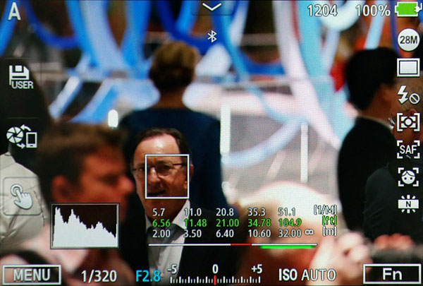
This shot also shows the uniquely well-executed focus-range control that's built into the forthcoming 300mm f/2.8 lens Samsung was also displaying at the show. To set the range, you slide the focus control switch on the side of the lens to the "set" position, and the camera shows both where it's currently focused (the red bar under the distance numbers), and the range that you've set (the green bar below the red one). You can adjust both the near and far ends of the focus range with the camera's control dials. Once set, slide the lens control to the "Custom" position, and the camera/lens will ignore subjects either closer or further than the range you've set. We've seen similar focus-control features before, but Samsung's seems more powerul and the user interface is very straightforward and intuitive.
The Samsung NX1's fast sensor readout, large array of focus pixels, and fast processor make for speedy subject-tracking AF. (As with other features, though, we'll obviously need to test this in the real world, before we can arrive at any firm conclusions.)
DE: So... faces and things like that too, or other objects?
JK: Face recognition is actually handled by a separate hardware block.
DE: Oh, really? So even in the previous DRIMe, there was hardware for face recognition.
JK: Right. So far we've only announced the baseball application, but they're working on other kinds of sports applications, too.
DE: Ah - other kinds of sports. So it's very much a sports application, but you're looking at other sports besides baseball that it would be useful for. That's really very interesting, it's an interesting feature.
[Samsung wouldn't give any hints of what other sports they might develop applications for, but I can easily imagine tennis, or the image of a ball coming off the golf club, etc.]
I wanted to come back to the data-readout speed. Is the camera actually capable of recording video at 240 frames?
JK: No.
DE: Oh, because the codec isn't fast enough to compress and format it?
JK: Actually, we just didn't implement that functionality, but the DRIMe V and the sensor could do it. When the guys in R&D were working on the Samsung Auto Shot feature, they recorded live 28 megapixel, 240 fps "video" to help with the debugging. We didn't see there being an application for that, at least for very, very few people.
DE: Yeah, 28 megapixels at 240fps is an awful lot of data; that high a frame rate probably wouldn't be very useful for still photographers, and there's no video format that big or fast...
Going back to the processor itself how has your noise reduction processing changed as a result of having so much processing power available? What has that allowed you to do that you couldn't do before the DRIMe V, in terms of the actual algorithms?
JK: The DRIMe V actually has a lot of IPs [small hardware circuit blocks] dedicated to noise reduction. It's pretty cool; there are a lot of them, and each one does a different type of noise reduction processing, all at the same time. The DRIMe IV didn't have these.
DE: Really? So all these IPs can all be working in parallel doing their own noise reduction, and then some higher-level processor can come in and say, "Oh this is this type of image content here, so I'm going to use the output from this IP, but over here there's different content, so I'm going to use the output from this other one"?
JK: Yeah, yeah.
DE: Wow, I don't know a lot about the details of image processors for digital cameras, but my impression has been that it was more software-driven. Here, though, all the different NR algorithms are being executed at the same time.
JK: Yeah, hardware's the only way to do this.
DE: Yeah. Wow, that's really interesting. And yet, because of Samsung's advanced processing, the power consumption is quite low. How does power consumption compare to DRIMe IV?
JK: It's actually a bit lower.
DE: It actually became lower, even though, even though there was such a huge jump in horsepower?
JK: Yeah, because it's a new semiconductor process for the DRIMe V.
DE: I think you said earlier that the DRIMe V had about twice the processing power, does that mean twice as many hardware units?
JK: Yeah. It's not just the number of units, though; with the 32nm design rules, there are a lot more gates in each processing unit.
DE: And how many regular CPUs are there?
JK: Five general-purpose cores.
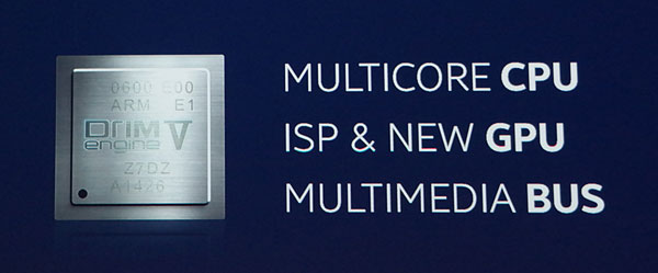
JK: Another important point is that the DRIMe V has the world's first HEVC codec. (aka H.265)
DE: Ah, yes. I was just about to ask about that. So it's also doing the H.265 encoding. And that's presumably also hardware, I would think.
JK: Right. If you check, I think it's the first HEVC codec in a camera. That makes it pretty amazing as well. H.265 is a lot more sophisticated than H.264; you can get similar image quality with only half the data rate.
DE: Ah, so for instance 100 MBits/s with H.265 is like 200 MBits/s with H.264.
JK: Yeah, pretty much. Another important thing is that the NX1 has a low-latency EVF.
DE: Latency, oh yeah, actually, I did want to ask that. So does that mean for viewfinder, because it says five milliseconds. So is that 200 frames a second?
JK: No, actually the display refreshes at about 54 fps, but the key thing is that the EVF and the sensor are sychronized. The two are genlocked, so there's always just a 5 ms lag between what's hitting the sensor and what's being displayed on the EVF's current scan line. I think we're the only ones who can do this.
DE: The video streaming through HDMI port, is that 4:2:2 on everything?
JK: It's 4:2:2 out the HDMI 1.4 port; it's 4:2:0 as it goes to the SD. And it's H.265 to the card for both HD and 4K, so whatever video mode you're saving to SD card, it's using H.265, so you're going to get much more efficient and better-quality HD out of it.
DE: What's the maximum bitrate to the card?
JK: I don't have a bitrate yet, but it's much more efficient compression. It requires more computing power to do it, but just as a rough example, I can run a Class 10 card through this, no problem. To do H.264 on, let's say, a competitive piece, I need a UHS-3 card.
DE: So it's really a whole different metric with H.265; you can't just directly compare megabits per second with data rates for H.264. It seems that 100 megabits here is going to be like 200 megabits there, so just looking at the data rate isn't going to translate directly into video quality.
JK: Right, right. The image quality for H.265's better. The noise reduction, or the compression artifacting is less, but it's twice as efficient in terms of space.
DE: That's about it for my questions, and I see we're also about out of time. Wow, that was sure a lot of ground we covered, thanks for the time and all the info!
JK: No problem!