Pixels for Geeks: A peek inside Nikon’s super-secret sensor design lab
posted Tuesday, July 17, 2018 at 12:56 PM EDT
I’ve known for some time that Nikon actually designs their own sensors, to a fairly minute level of detail. I think this is almost unknown in the photo community; most people just assume that “design” in Nikon’s case simply consists of ordering-up different combinations of specs from sensor manufacturers, picking a feature from column “A”, another from column “B” and so on, like a Chinese restaurant menu. In actuality, they have a full staff of sensor engineers who design cutting-edge sensors like those in the D5 and D850 from the ground up, optimizing their designs to work optimally with NIKKOR lenses and Nikon's EXPEED image-processor architecture.
Given my own background in the semiconductor industry (my Master’s Degree is in semiconductor physics, although I haven’t practiced as an engineer for many years now), I’ve always wanted to do a story about sensor design, and it seemed like telling the largely-unknown story of Nikon’s sensor design abilities would be a good backdrop for it.
A chance to peek behind the curtain?
I’ve approached other sensor makers in the past about doing a story on sensor design, but it’s such a proprietary area that I’ve always been turned down flat. In Nikon’s case, though, I thought they might be interested in having the story told, because it’s a unique ability of theirs, compared to many of their competitors. I thought it would be beneficial to them to have more people be aware of it, and it might be an angle for me to finally get sensor engineers to peel back the curtain, if only a little.
And from our reader’s side, given that the D850 won our Camera of the Year award for 2017 and its sensor recently receiving the first DxO Mark score of 100 for an SLR, I thought there’d be a lot of interest in hearing some of what went into its making.

So I pitched Nikon on the idea of doing a sponsored article about their sensor-design efforts. As with others I’d approached in the past, they had a lot of concern about the deeply proprietary information and technology involved. It took a good four or five months of discussion and back and forth, and the strong support of Nikon’s US PR and marketing team, but in the end they agreed, resulting in the story you see here.
There’s a lot to talk about, so this will be a very long article, but I hope readers will find it as interesting to read as I did to research and write it.
We obviously won’t be able to get all the way down into the details, but hopefully this overview will shed some light on what it takes to make a great-performing sensor, and show some of the surprising (to me, at least) ways in which Nikon optimizes their sensor designs.
What exactly do Nikon’s sensor designers do?
Even though I knew that Nikon had its own sensor design operation, I was surprised to learn just how deep the process runs.
Companies designing chips of whatever sort generally rely on standard processes established by the “foundry” company that does the actual manufacturing. In these cases, the design process is “just” a matter of defining the layout of the devices on the chip. I say “just” though, because it’s far from a routine process to do this. The size and shape of transistors, photodiodes, resistors and capacitors determines their electrical characteristics, and there are loads of tradeoffs involved in balancing light-gathering efficiency, noise levels, readout speeds, on and on. A big trick is designing the pixels and readout circuitry so there’s as little “dead” (non-light-sensitive) area as possible, while maintaining readout speeds and minimizing power consumption.
This is what Nikon does, but their design and simulation extends to an incredible level of detail.

Prior to my tour, I had no idea Nikon’s engineering extended as deep as it does. Some of that is just a result of the many years since I was actively involved in the semiconductor industry, but the level of design, simulation and testing I saw was frankly astonishing.
Why design an original sensor?
It’s is a fair question: Commodity sensors (ones you can just buy from a sensor manufacturer’s catalog) are really quite good these days, so why would Nikon make the huge investment to design their own from the ground up?
I asked about this, and it turns out there are a number of reasons, many having to do with being able to optimize the camera system as a whole, in ways that you can’t if you’re just using off-the shelf parts.
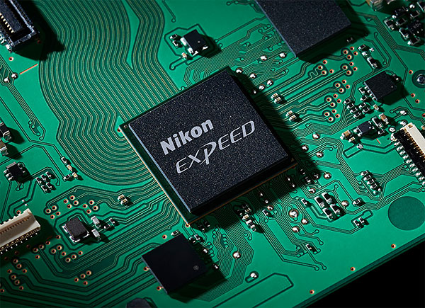
In answering my question, Sanbongi-san talked in part about the need to match sensor designs to the capabilities of Nikon's EXPEED image processing engines (which are also designed in-house), and about being able to tailor performance to the level of camera each sensor will be used in.
Another surprise for me, though, was the extent to which he talked about matching sensor designs to the characteristics of NIKKOR lenses. As we’ll see later on, they place a lot of emphasis on this, and do a lot of testing to optimize the overall combination of lens, camera and sensor from an optical standpoint.
Finally of course, doing their own R&D lets them create sensors like the one in the D850, with its low-ISO ability (a true ISO 64), and the one in the D5, with its exceptional light sensitivity and quantum efficiency. (The efficiency of converting incoming light to an electrical signal.) Throughout all our discussions, image quality was a recurring theme, whether expressed in terms of dynamic range, noise levels, interactions with NIKKOR lenses or color accuracy.
Image Sensors 101
Before we get into the details of what Nikon does, it’d help to understand a bit of what goes into an image sensor, what its component parts are, and how it connects to the outside world.
(Note that much the following is greatly simplified. For our more knowledgeable readers, feel free to add your thoughts in the comments at the bottom, but please understand that I’ve done my best to tell the basics without getting too mired in the details…)
Light is photons
Most people have at least heard of photons, the elemental particles of light. We’re never aware of them in daily life, because they’re far too small for our eyes to see individually. What we perceive as light is many (many) billions of photons hitting our eyes at once. (One estimate is that when we’re looking at a clear blue sky, about 3 x 10^14 photons per second are entering each eye. That’s 300,000,000,000,000, or 300,000 billion photons per second!)
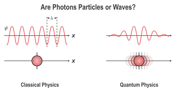
Brighter or dimmer light just means more or fewer photons. As we reduce the number of photons/second, at some point we see nothing at all. But far beneath our perception of smoothly-varying brightness are individual light particles, the photons.
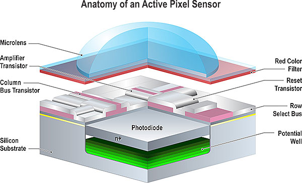
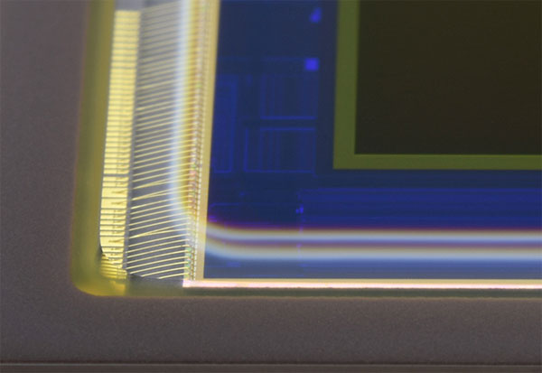
To record light, image sensors need to somehow convert photons to electrical signals, measure those signals digitally, and pass the information on to the camera’s processor. This involves five elements; the microlenses, photodiode, readout circuitry, analog to digital (A/D) converters and data transfer circuits. Let’s look at each one separately.
Catch all the light: The microlens
The sensor can only “see” photons that hit its light-sensitive areas, and some of the space in each pixel has to be dedicated to other functions, to measure and read out the light collected. (Even in so-called backside-illuminated sensors like the one in the Nikon D850, there are still isolation areas between pixels that aren’t light-sensitive.)
To make the most of the available light, modern image sensors have “microlenses” above each pixel, that collect the incoming light and focus it on the light-sensitive area beneath. There are a lot of tricks to optimizing microlens design, including so-called “gapless” layout, the position and even shapes of the microlenses themselves.
As part of matching their sensors to NIKKOR optics, Nikon’s sensor designers pay a lot of attention to the microlenses and the structures between them and the silicon surface. Like essentially all camera sensors today, Nikon’s microlenses are offset a variable amount relative to the pixels beneath, to compensate for light rays arriving at oblique angles near the edges of the array.
Interestingly, Sanbongi-san noted that it’s not just current-day NIKKOR optics that are considered; they extend their optimization a little outside the parameters required by their current lenses, to allow for future development.
Photons in, electrons out: The photodiode
Once we’ve collected as much of the light falling on the sensor as possible, the next step is to convert photons into electrons (the fundamental particle of electric charge), so they can be measured electronically. This is the job of the photodiode.
The underlying process is pretty basic: Whenever a photon is absorbed in silicon (the material the sensor is made of), it kicks out an electron. At the heart of every pixel is a photodiode, an electrically-isolated area that collects the electrons generated during an exposure.
Because everything begins with the photodiode, its characteristics have a profound effect on image quality. In simple terms, we want two things from the photodiode.
The challenge of low ISO, and why it’s important
First, at the bright end of things, we want the photodiode to be able to hold lots of charge without “saturating” (ceasing to respond to more light). This basically sets the minimum ISO we can use a sensor at; if the photodiodes fill up quickly (that is, when they’re exposed to less light), the minimum ISO is higher. This is very similar to how film behaved: Once you hit maximum exposure, the negative won’t get any darker or the transparency won’t get any clearer. This happens at lower light levels with higher-ISO films than with lower-ISO ones. The same is true of sensors.
It’s probably no surprise that, generally speaking, big photodiodes can store more charge than tiny ones. This is the reason that we now often see minimum ISO ratings of ISO 200; the tiny pixels of modern sensors can’t store as much charge as the larger ones of days gone by. (Again, this is greatly simplified; I ask our more knowledgeable readers to bear with me here :-)
While a minimum ISO of 200 isn’t an issue if you’re shooting at smaller apertures or in lower light, it’s a real issue if you’re trying to shoot at wide apertures in bright light, or to use slower shutter speeds to achieve motion blur. Of course, you can always use an ND filter in such situations, but they’re a nuisance, especially if you’re using multiple lenses, and want to switch back and forth between tack-sharp and creatively blurred shots.
This is one area where Nikon’s dedicated sensor design has paid off for them: The D850 has the first true ISO 64 capability in an SLR. (Other cameras have special “Lo” ISO settings that will get there, but those come at the expense of poor tonal qualities and blown highlights.) Sanbongi-san told me that they developed the D850’s true ISO 64 capability in response to requests from motor-sports shooters, who wanted to shoot at large apertures and slow shutter speeds, so they could pan to follow the race cars while dramatically motion-blurring the background.
I don’t know enough about sensor design to understand the details of what’s involved, but when I asked Sanbongi-san what his team’s proudest achievements were, he mentioned the D850’s true ISO 64 first.
No Snow: Leaky pixels = stuck pixels!
At the other end of the scale, when there’s very little light, we want to make sure that the only electrons in the photodiode got there as a result of incoming photons. It turns out that photodiodes “leak” charge, letting random electrons creep in from the surrounding silicon. This shows up as “hot” pixels that look bright whether light is falling on them or not. Even if a given pixel doesn’t stand out on its own, random charge leaking into a sensor’s pixels from this so-called “dark current” can be a significant cause of image noise.

(Again, to our more knowledgeable readers, yes, shot noise is a big part of high-ISO noise, and there’s nothing to be done about that at a sensor level; it’s just math. But minimizing both bulk and surface leakage while maximizing well capacity and maintaining high readout speed is a significant challenge.)
Sanbongi-san pointed to the D5’s sensor as a case where they’d maintained excellent quantum efficiency and very low leakage, while still maintaining high readout speeds.
Charge to volts: The readout circuitry
After a shot’s been taken, the next step is to convert the electrons collected by the photodiode into a voltage that can be read out. This is the job of the readout circuitry. The readout circuits are basically little electronic amplifiers that turn the collected charge into a voltage, with additional electrical switches and wires to bring the resulting voltages to the next step of the process, which is…
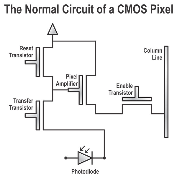
Volts to bits: The A/D converter
Computers understand 1s and 0s, not voltages, so we need to convert the voltage from the readout circuit into a number that the image processor can understand. This is the job of the analog to digital (A/D) converter or ADC.
This is a particularly critical part of the process, as the analog to digital conversion needs to happen very quickly, as well as very accurately. The A/D converters in Nikon’s sensors measure the pixel voltages with a resolution of 14 bits. That translates to an accuracy of one part in 16,384!
This is an area where there have been huge strides in sensor technology over the last 10 years or so. Once upon a time, sensors just fed analog voltages to external A/D converters in the body of the camera. This was not only slow, but a source of noise, as the wiring between the sensor and the camera could pick up a lot of electrical noise from other parts of the camera’s circuitry. Eventually, A/D conversion moved on-chip, avoiding noise pickup from the analog wiring to the camera. This wasn’t simple to do, though, as the semiconductor processing that’s ideal for a sensor is far from ideal for A/D and digital circuitry. It was hard to get fast, accurate A/D conversion built into the same chip as the sensor.
Once the A/D circuitry was moved onto the sensor chip, the next innovation was massively parallel A/D conversion, with a separate A/D converter for every column of pixels in the array(!) This is where we’re at today. For obvious reasons, Nikon would prefer not to discuss fine details, but as far as I know, most sensors today use per-column A/D conversion.
Bits out to bits in: The data transfer circuitry
The final step is to transmit the numbers measured by the A/D converters to the image processing engine. The trick here is getting the data to the processor fast. In the case of the D850, with 45 million pixels, 14 bits per pixel and 9 frames/second with the accessory grip, that amounts to 5.7 billion bits per second, or 716 megabytes/second. That’s a serious load of data.
Achieving these kinds of data rates requires special technology, called LVDS, for “Low-Voltage Differential Signaling”.
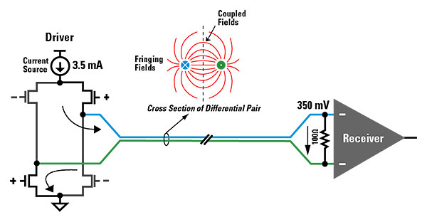
Image provided by Dave at ti under a CC BY-SA 3.0 license via Wikimedia Commons.
(Knowledgeable readers: Yes, LVDS refers to a specific interface standard for flat panel displays, but it’s also a generic term, which is the sense in which I’m using it here.) Signal levels in LVDS are very small, so it’s easy to drive connections at extremely high speed. The “differential” part means the information travels on a pair of wires, and only the difference in voltage is significant. This minimizes noise effects from the signal transmission.
Here was another big surprise for me: I’d just assumed that the connection between chip and processor would be a simple matter of 1s and 0s. In practice, the data transmission rates are so close to the limit of what’s possible that Nikon uses proprietary encoding to make sure that all the bits make it across with 100% reliability. I had no idea that camera sensors pushed the technology so hard in this area.
This ultra high-speed communication is part of why Sanbongi-san made such a point of matching their sensors to the EXPEED processors. The number, speed, and characteristics of the communication channels between the sensor and processor are integral parts of the overall system design.
Life in the trenches
I was curious how Nikon organizes its sensor-design efforts. Do they have experts that focus on specific areas (pixel design, A/D, etc), consulting with teams for individual sensor designs, or do they do something different?
It turns out that all of Nikon’s sensor engineers work in teams on specific sensors. Some people are experts or have more experience in certain areas, so they’ll help out other teams that might be having a problem in their area of expertise. But on a day to day basis, everyone is working on the design of a specific sensor, along with others on that chip’s team. (So there was a D850 sensor team, a D7500 one, etc.)
Once a week, there’s an all-hands meeting of the entire team, where the prior week’s progress is discussed, and new objectives are set for the week to come. From there, the individual teams among themselves on whatever the priorities are for that week.
Development: It starts with a camera
I was curious what sensor development looks like at Nikon - how does it get started? Do they work on developing new circuits and technology, and then just build them into new sensors as they’re available? Do they design future cameras based on what they believe is coming in terms of sensor capabilities. What’s the starting point?

Unlike a commodity sensor company, Nikon begins by deciding what sort of camera they’re going to build, what market it will serve, and the price point they need to hit. Feedback from their real-world users drive camera development, and the sensor designs flow from there.
While their efforts are always organised around specific camera models, Nikon’s sensor R&D goes on more or less continuously. I asked Sanbongi-san how long it takes to develop a sensor, and he said that, while it’s hard to point to a specific moment in time as the starting point for any given sensor, the process takes multiple years for advanced sensors like those in the D5 and D850.
Early stages: process and device simulation
As noted earlier, sensor fabrication takes a long time (typically months from start to finish), and is crazy-expensive, so you have to really pick your shots.
It’s been years since I was involved in the semiconductor business myself, so I was completely blown away by how capable and detailed the simulation software has become. You can basically set up an entire semiconductor factory in the CAD software, with the computer simulating every step of the fabrication process down to an atomic level. Decades of development by third-party companies has resulted in simulation software of unprecedented capability. (I’m not sure which company’s simulation software Nikon uses; there are no less than four different companies marketing a product called “TCAD” :-)
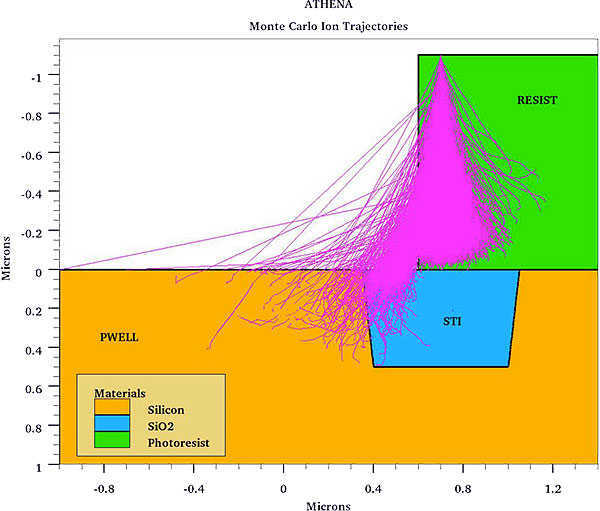
It’s hard to convey just how insanely detailed the CAD simulations of the semiconductor processing are. One minor example: To make semiconductor devices, you introduce tiny amounts of impurities into the silicon, to change its electrical properties. These days, this is done by using room-sized particle accelerators to smash impurity atoms into the silicon at very high energies. In sensor manufacturing, it’s not uncommon for these “ion implanters” to operate at energies of a million volts or more(!)
But a lot can happen on the way from the accelerator into the silicon, so the simulation software traces the paths of individual impurity atoms, as they smash through the photoresist, refract through the edges of it, and reflect off other structures. Trace a hundred thousand particles or so and you’ll have a pretty good idea of what things look like in the silicon afterwards. But this is just one small part of the overall process; the level of detail is truly mind-boggling.
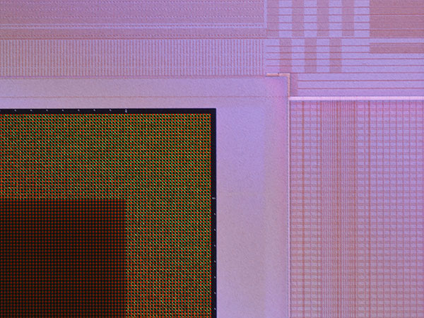
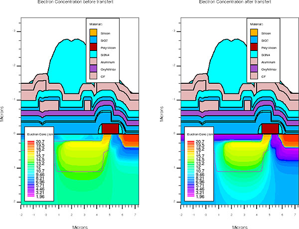
Once the process-simulation software has created a three-dimensional model of the sensor in the computer, you can then simulate its operation, again to an unbelievable level of detail. As we saw in one of the illustrations above, you can throw simulated photons at the sensor model, trace their paths until they’re absorbed by the silicon, and model the resulting charge distribution and voltage levels at a nano-scale. The amplification and readout process is likewise simulated in three dimensions, nanosecond by nanosecond, based on the fundamental physics.
A little later: Dedicated test wafers
Computer simulation plays such an important role because actually fabricating sensor chips is an incredibly expensive and time-consuming process. You don’t get a lot of shots at making the chips themselves, so you need to really make them count.
This was another area that surprised me: Previously, I thought that new test circuits were just run alongside normal production lots, so you could test new circuit designs on an ongoing basis.
Surprisingly, Sanbongi-san told me that Nikon sometimes runs dedicated silicon wafers, just to test their new circuitry. I guess this makes sense, since at least some of their designs depend on custom processing that the chip foundry wouldn’t normally run. But wow, this is a major expense and commitment; custom semiconductor processing is very, very expensive!
Most people have no idea how long it takes to produce finished sensors, starting from the raw wafers. It’s a long, long process, easily taking 4 or even 5 months, from start to finish. While Sanbongi-san said it’s possible to slightly accelerate processing on some batches of test wafers, there’s ultimately no way around the fact that it takes months to go through all the hundreds of individual steps involved in fabricating sensors.
I was curious what form the test circuits take: Do they just make isolated circuits, a pixel here and there, or isolated amplifier circuits, for example?
It turns out they usually test new pixel circuitry by dividing a sensor array into multiple sections, each implementing a new pixel design, with thousands of pixels in each. So a single test array may have pixel circuitry for upwards of 50 or 60 different design variations in it. They do sometimes test individual, smaller circuits, but most of the time, they process entire test arrays, with thousands of pixels in each block.
Given the length of sensor R&D cycles, there are multiple sensors under development at any given point in time, so many different circuits need to be tested alongside each other. I found it interesting that test circuitry for very different cameras might be run together, on the same set of test wafers. This was very different than what I’d expected; yet another interesting factoid I picked up on this tour.
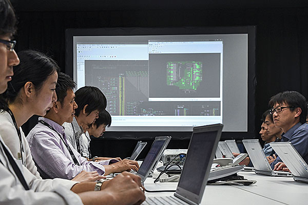
Testing, testing and more testing…
As you might expect, testing is a critical part of sensor development, and I saw ample evidence of this in Nikon’s labs while I was there. It’s not just a matter of what the sensors do on their own, but also a question of how they interact with NIKKOR optics and in the camera system as a whole.
While most camera companies do extensive optical testing of their cameras and lenses, Nikon’s sensor-development team has to go a lot deeper, to evaluate not only raw sensor performance, but how the sensors interact with the cameras and lenses they’re used in and with as well.
This involves not only optical testing of various sorts, both with and without lenses attached, but also extensive electrical and photo-electrical testing across a wide range of temperatures, to insure that the sensors will perform under the extreme conditions professional users expect their Nikon cameras to stand up to.
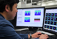
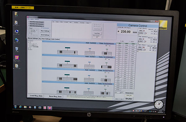
The sheer amount of data that has to be processed to support these evaluations is pretty staggering. Sanbongi-san said that routine testing involves literally tens of thousands of images for each sensor design. Multiply that by the range of sensors they produce and the need to evaluate multiple iterations of each new design, and it adds up to a lot of number-crunching, not to mention the amount of time it takes to collect all that data, even with automated systems.
While many parts of Nikon’s sensor testing were too proprietary to show us, even under a stringent non-disclosure agreement, we did get to see four sets of tests that give some idea of the depths Nikon goes to in evaluating new sensor designs.
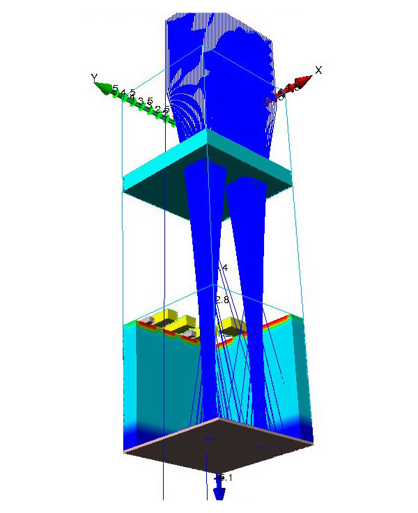
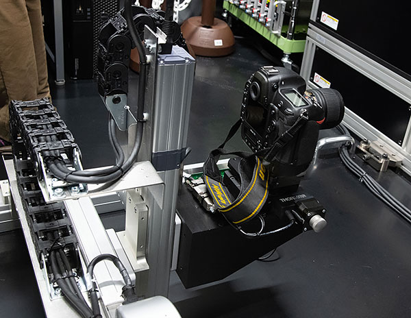
Full-system flare testing
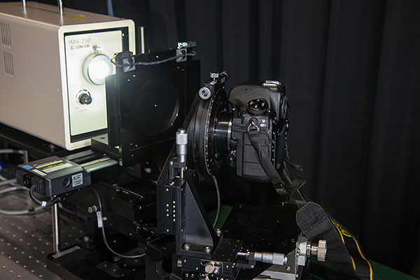
This is a system Nikon uses to evaluate internal reflections and optical crosstalk that can result in flare or “ghost” images in the presence of extremely bright light sources. (Think of the sun in the corner of the frame.) The system sweeps an extremely(!) bright LED light source past a camera with attached lens held in various positions and orientations. The test tries to capture all possible angles and positions of the light source relative to the camera, so a lot of shots are required for each test.
The point here is that there are a lot of chances for things to go awry when you have light rays striking the sensor from very oblique angles. The entire stack of sensor, microlenses, package cover glass, low-pass/infrared filter of the camera and the attached lens interact with each other. This apparatus lets the sensor engineers test different configurations of the microlenses and packaging variations, to find and fix artifacts of this sort while the sensors are being designed.
I heard a lot during the interview and tour about how much effort the sensor design group puts into optimizing performance with NIKKOR optics. I hadn’t really thought about this much in the context of sensor design, but it makes sense: We tend to think of the sensor, camera and lenses as entirely separate elements, but of course they’re all part of a complex optical system that turns the light from a subject into 1s and 0s in a digital file. It’s not just a question of how well each of the parts works on its own, but how well the combination works together.
Prior to this tour, I’d never stopped to think about how the lens, the camera’s optical low pass and infrared filters, the microlenses on the sensor’s surface and even the interface between the microlenses and the silicon surface beneath all interact with each other. As described further below, this interaction can be critical in controlling optical crosstalk (the tendency for light falling on one pixel to bleed over into adjacent ones) that causes some forms of “banding”.
In the test shown above, the sensor is put in a camera body with an attached lens, mounted on a computer-controlled stage. The stage can move right/left, up/down, and in/out relative a light source, and the camera can be rotated to different angles as well.
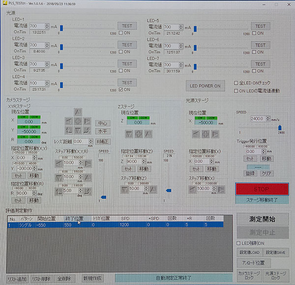
The computer system steps the camera through a range of positions and orientations, and for each one, a sled with a very bright LED light source sweeps across in front of the camera/lens combo. (The light was extremely bright when we saw it, and the technician said it was turned way down compared to how bright it is when the test is actually being run; it must be almost blinding then.) This is repeated over and over, to cover every possible position and angle of the light source relative to the camera and lens. A computer analyzes the results of hundreds of runs with each lens to characterize the degree to which ghosting appears, so different sensor designs can be compared across a range of lenses.
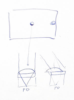
Angle of incidence testing
The system shown above evaluates how the combination of the camera’s low pass/infrared filter and the sensor’s microlenses respond to light coming from different angles. A high-intensity illuminator and tiny aperture create a point-source of light in front of the camera. The computer then rotates the camera through a range of positions, so light from the point source can strike the sensor from a full range of angles. As before, a computer both controls the system and analyzes the sensor’s output. (When a test is being conducted, the camera and aperture are draped with heavy black cloth, so the only light hitting the sensor will be that coming from the tiny aperture.)
Understanding the optical behavior of the microlenses, particularly how they handle light rays arriving from different angles is a key part of integrating a sensor into a camera/lens system. In camera systems, light rays hitting the center of the sensor fall almost vertically, while those striking the edges can be at fairly low angles.
At the simplest level, microlenses centered over each pixel would misdirect light coming from a low angle, causing much of it to miss the light-sensitive area of the pixel. To compensate for this, Nikon (and most sensor makers) shift the the microlenses at the edges and corners of the array inwards, so all the incident light will make it to the silicon surface.
From our discussions, it sounded like this shifting of the microlenses is only a small part of what Nikon does to control the optical characteristics of the sensors. Full details would both be very technical and highly proprietary, but I can imagine some of what's involved. It turns out that the surface of a sensor is a complex 3-D structure that can be surprisingly tall relative to the pixel area itself. This makes it tricky to get the maximum amount of light from the tops of the microlenses all the way down into the “canyons” formed by metallization and other surface structures. - And I’m sure there are issues with internal reflections, minimizing the amount of light absorbed by the walls of the canyons, etc, etc.
The whole issue of how the sensor pixels handle off-axis light rays is a critical issue in the design process. Hence the need for a machine like the one above, to be able to fully characterize angle of incidence-related behavior.
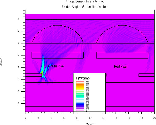
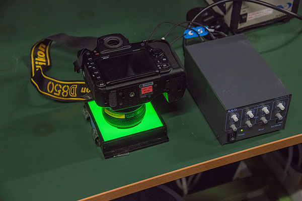
RGB testing
The simple device shown below is used to check the RGB response of the sensor. Narrowband LED light sources behind a thick diffuser let the operator precisely adjust how much of each color is emitted, to evaluate the performance of the filters in the sensor’s color filter array, and the net response of the combined sensor/microlens/color filter array/low-pass and IR filter system to light of different colors. This simple instrument lets Nikon measure color cross-talk, which is the extent to which pixels of one color respond to other colors of light. (For example, how much a red pixel responds to green or blue light.)
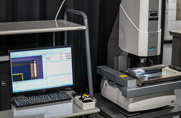
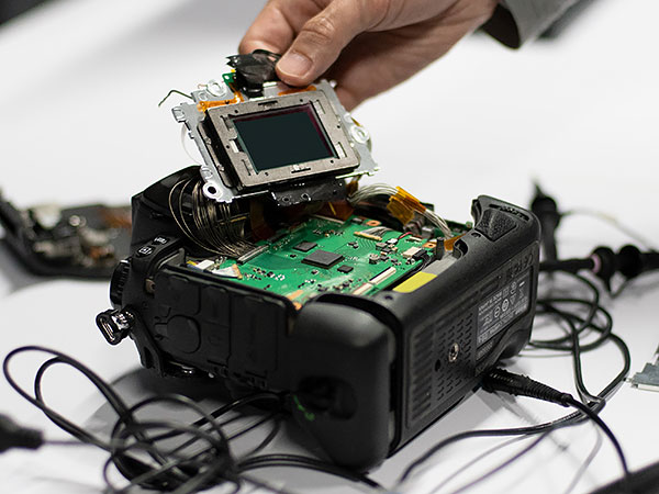
Circuit testing
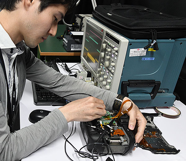
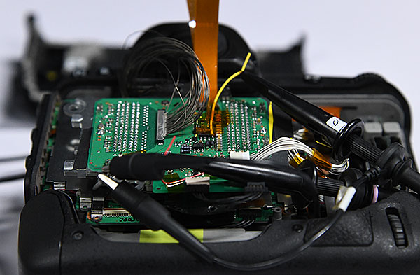
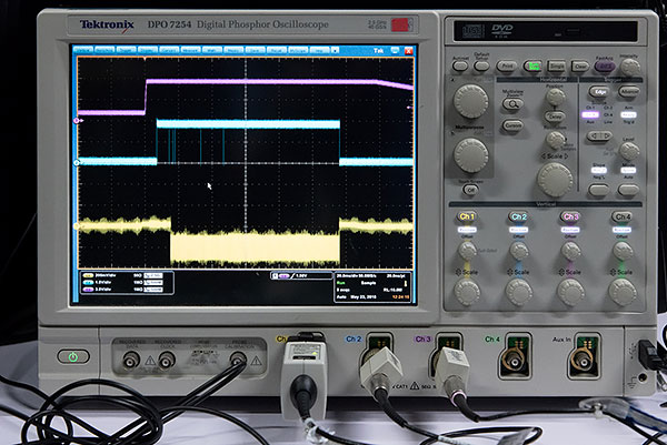
The three tests above all involved the sensor’s optical properties, but of course there's an electronic side as well, that has to interface with the camera’s processor. Complex “breakout boards” allow access to what would normally be internal signals. The shot below shows a breakout board attached to a D5 camera body. There’s a lot to interface with; I count 180 solder points on this board that I assume are connected to the sensor package.
What does the future hold?
At the close of our time together, I asked Sanbongi-san what he thought the future held. Have we reached the limits of silicon? What sorts of things might we see in the future? Specifically, what about quantum dot technology that’s become something of a buzzword lately?
He agreed that we’re approaching physical limits with silicon sensor technology, but felt that there’s still room for advancement, to improve quantum efficiency and dynamic range, and in reducing readout noise. Beyond that, who knows? There’s the possibility of some sort of “avalanche” technology that would multiply the number of electrons generated by each photon, although that would also increase noise levels significantly. Perhaps multi-shot/image stacking technologies can be more broadly applied than they are presently, in very low-light situations? As for quantum dots, he thought that those were still quite a ways in the future, at least in terms of practical multi-megapixel sensors.
While we’re ultimately limited at the low-light end of things by the fact that we’re basically counting individual photons, under bright conditions, there are still advancements to be found, as they did with the ISO 64 capability of the D850’s sensor.
Of course, he obviously couldn’t comment on anything that Nikon actually has under development, so it’s understandable that his replies were a little circumspect. I’ll be waiting along with the rest of you, to see what he and the Nikon sensor engineering team come up with next.
A thank-you
I enormously appreciate the amount of time and effort Sanbongi-san, his engineers and the entire Nikon staff devoted to this project; I could tell that there was a tremendous amount of preparation involved, and I spent literally hours talking with him and asking questions. Then there’s the leap of faith it took for Nikon to give an outsider access to such an incredibly sensitive area of their operations.
We've been wanting to do an article about sensor design for a long while now, and are so happy to have finally gotten the chance. It required an enormous investment of time and effort on our part to bring to fruition, let alone the unprecedented access Nikon Corporation gave us to extremely proprietary areas of their operation. Let us know in the comments if you like this sort of deep dive into behind-the-scenes technology: It was a huge effort, but we're happy with the results, and hope you will be as well!
Thanks to Nikon for sponsoring the creation of this article.
• • • • •
Want another tour?
• Glass for geeks: An in-depth tour of Nikon’s Hikari Glass factory •