
Sony and TSMC Team Up to Develop Next-Generation Image Sensors


Imaging Resource is reader-supported. When you buy through links on our site, we may earn an affiliate commission. How this works.
Sony and Taiwan Semiconductor Manufacturing Co. (TSMC) are joining forces to develop the next generation of image sensors, with mass production targeted for 2029. The project will be based in Kumamoto Prefecture in southwestern Japan and represents a multi-billion-dollar push into advanced imaging technology.
According to Nikkei Asia, the two companies are investing a combined $6.3 billion in the initiative. Sony will hold a 60% stake in the joint venture, while TSMC will own the remaining 40%.
For Sony, the scale of the investment is particularly significant—roughly three times the profit generated by its image sensor business in its most recent fiscal year.
A Major Investment in Image Sensors
Sony and TSMC first reached a basic agreement on their collaboration in May, outlining plans to jointly develop next-generation image sensors. The finer details are still being finalized, with the joint venture expected to be formally established by the end of Sony’s 2026 fiscal year in March 2027.
The partnership will center on an existing Sony Semiconductor Solutions facility in Koshi, Kumamoto, where the companies plan to build large-scale R&D operations and new production lines. The two firms are also in discussions with Japan’s Ministry of Economy, Trade and Industry regarding potential government subsidies to support the project.
Both Sony and TSMC have remained tight-lipped about further details. TSMC has said there is no additional information beyond its initial May announcement.
Building Sensors for Smartphones and AI
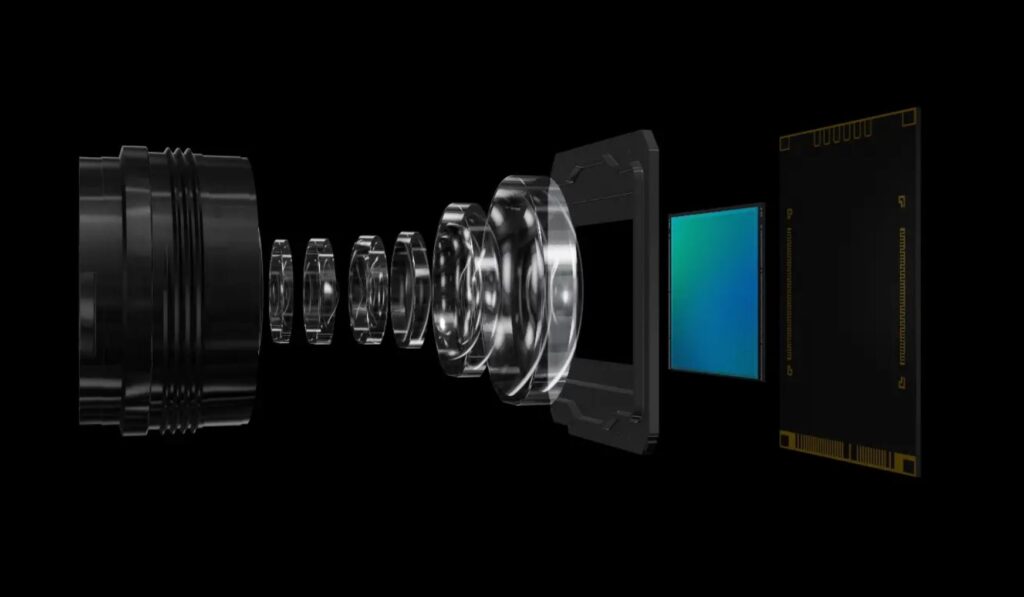
The Sony and TSMC partnership aims to produce sensors for Apple iPhones.
A key focus of the partnership is the development of high-performance image sensors for smartphones, including future iPhone models.
However, the ambitions go well beyond traditional mobile photography. The new sensors are expected to significantly enhance how artificial intelligence systems interpret visual data, particularly in the emerging field of “physical AI.”
Physical AI refers to systems that interact directly with the real world, such as robots and autonomous vehicles. In these applications, advanced image sensors capable of capturing richer and more accurate visual information will play a critical role.
Shinji Sashida, President and CEO of Sony Semiconductor Solutions, described the collaboration as a way to combine both companies’ strengths to accelerate the development of next-generation imaging technology.
What About Apple’s Own Image Sensors?
Apple and Samsung have also announced plans for a U.S.-based facility focused on semiconductor development, sparking speculation that Apple may be working on its own advanced image sensors, including a rumored triple-layer design for future iPhones.
However, this does not necessarily mean Apple would move away from Sony sensors entirely.
In practice, smartphones often use components from multiple suppliers, and even different camera modules within the same device can rely on different sensors. Manufacturers also frequently mix sensor technologies across product lines and price tiers.
As a result, Apple could potentially adopt its own sensor technology while still using sensors produced through the Sony-TSMC partnership.
Sony Aims to Strengthen Its Market Lead
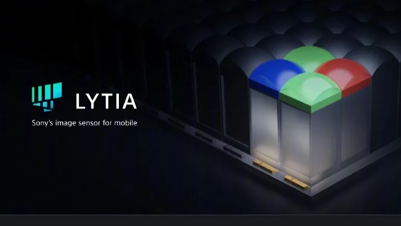
Sony’s Lytia image sensor brings LOFIC technology to smartphones.
Sony currently dominates the global CMOS image sensor market, holding more than half of the share according to the report.
Still, competition is intensifying. Companies such as China’s OmniVision and South Korea’s Samsung Electronics are investing heavily to expand their own image sensor capabilities.
Against this backdrop, the partnership with TSMC appears to serve a dual purpose: advancing sensor technology while also reinforcing Sony’s leadership position.
Sony contributes decades of expertise in image sensor design, while TSMC brings world-leading semiconductor manufacturing capabilities. Together, the companies aim to stay ahead in a market that is rapidly expanding beyond traditional photography into AI-driven applications.
What Could Come From Kumamoto?
Mass production from the new facility is not expected until around 2029, meaning the first products are still several years away.
As a result, it remains unclear exactly how these sensors will ultimately be used in consumer devices. However, the scale of the investment strongly suggests Sony sees major long-term opportunities in next-generation imaging.
For photographers, the most interesting question is whether any of this technology will eventually make its way into dedicated cameras. Given Sony’s role as a major supplier of sensors to the broader camera industry, innovations developed through this partnership could eventually benefit a wide range of imaging products.
For now, the Kumamoto project stands as a significant bet on the future of imaging—one increasingly shaped by computational photography, artificial intelligence, and machine vision.
More in News
 NewsArtizlab Recreates a Leica Classic 50mm Lens for Just $39910 Nov 2026
 NewsAdobe Expands Photoshop AI Tools and Adds Glow Effects to Lightroom10 Nov 2026
 NewsMitakon Speedmaster 45mm F1.4 Launches for Fujifilm GFX and Hasselblad XCD9 Nov 2026
 NewsPanasonic Registers New Camera in China, Sparking Lumix Announcement Rumors9 Nov 2026
 NewsSirui Expands Aurora Series With Two New Wide-Angle Prime Lenses9 Nov 2026
 NewsNikon May Have Accidentally Leaked the Upcoming Z706 Nov 2026